NCP5006EVB ON Semiconductor, NCP5006EVB Datasheet
NCP5006EVB
Specifications of NCP5006EVB


Related parts for NCP5006EVB

NCP5006EVB Summary of contents
Page 1
NCP5006 Compact Backlight LED Boost Driver The NCP5006 is a high efficiency boost converter operating in current loop, based on a PFM mode, to drive White LED. The current mode regulation allows a uniform brightness of the LEDs. The chip ...
Page 2
V bat GND GND 3 FB NCP5006 R1 D6 GND 15 W LWT67C Figure 1. Typical Application Thermal Shutdown 4 EN 100 k GND − 300 k +200 mV Band Gap Figure 2. ...
Page 3
PIN FUNCTION DESCRIPTION Pin Pin Name Type 1 V POWER out 2 GND POWER 3 FB ANALOG INPUT 4 EN DIGITAL INPUT 5 V POWER bat NCP5006 Description This pin is the power side of the external inductor and must ...
Page 4
MAXIMUM RATINGS Rating Power Supply Output Power Supply Voltage Compliance Digital Input Voltage Digital Input Current ESD Capability (Note 1) Human Body Model (HBM) Machine Model (MM) TSOP−5 Package Power Dissipation @ T = +85°C (Note 2) A Thermal Resistance, ...
Page 5
ANALOG SECTION (Typical values are referenced to T temperature, unless otherwise noted.) Rating High Level Input Voltage Low Level Input Voltage EN Pull Down Resistor Feedback Voltage Threshold Output Current Stabilization Time Delay following a DC/DC Start−up, = 3.60 V, ...
Page 6
Basically, the chip operates with two cycles: Cycle #1: time t1, the energy is stored into the inductor Cycle #2: time t2, the energy is dumped to the load The POR signal sets the flip−flop and the first cycle takes ...
Page 7
f(V out bat 1200 3 LED 1000 2 LED 800 5 LED 600 400 200 out bat (V) bat Figure 5. ...
Page 8
Output Current Range Set−Up The current regulation is achieved by means of an external sense resistor connected in series with the LED string The current flowing through the LED creates a voltage drop across the sense resistor R1. ...
Page 9
Output Load Drive In order to optimize the built−in Boost capabilities, one shall operate the NCP5006 in the continuous output current mode. Such a mode is achieved by using and external reservoir capacitor (see Table 1) across the LED. At ...
Page 10
Yield = f mA/L bat out 100 2 LED/ LED/ LED/ LED/ 2.50 3.00 3.50 4.00 4.50 V ...
Page 11
NCP5006 TYPICAL OPERATING WAVEFORMS = 22 mH, 5 LED, I Conditions 3 bat out Figure 20. Typical Power Up Response V out Inductor Current = 22 mH, 5 LED, I Conditions 3 ...
Page 12
NCP5006 TYPICAL OPERATING WAVEFORMS = 22 mH, 5 LED, I Conditions 3 bat out Figure 22. Typical Inductor Current = 22 mH, 5 LED, I Conditions 3 bat out Figure 23. Typical ...
Page 13
NCP5006 TYPICAL OPERATING WAVEFORMS Test Conditions mH mA, V out Figure 24. Typical Output Peak Voltage 92.00 90.00 ESR = 0.3 W 88.00 86.00 84.00 ESR = 1.3 W 82.00 80.00 78.00 3 3.5 ...
Page 14
Figure 26. Noise Returned to the Battery Test Conditions 3 bat Figure 27. Relative EMI Over 100 kHz − 30 MHz Bandwidth NCP5006 10 100 FREQUENCY (MHz mA, ...
Page 15
TYPICAL APPLICATIONS CIRCUITS Standard Feedback The standard feedback provides a constant current to the LED, independently of the V supply and number of LED bat GND R1 GND 15 W Figure 28. Basic DC Current Mode Operation with Analog Feedback ...
Page 16
Average Network R2 PWM 150 k GND NOTE: RC filter R2 and C3 is optional (see text) Figure 29. Basic DC Current Mode Operation with PWM Control To implement such a function, let consider the feedback input as an operational ...
Page 17
Digital Control Due to the EN pin, a digitally controlled luminosity can be implemented by providing a PWM signal to this pin (see Figure 31). The output current depends upon the Duty Pulse R1 GND 22 W NOTE: Pulse width ...
Page 18
NCP5006 Figure 33. Operation @ PWM = 10 kHz 25% Figure 34. Magnified View of Operation @ PWM = 10 kHz 25% http://onsemi.com 18 PWM V out VFB PWR CLK PWM V out PWR CLK ...
Page 19
Figure 35. Output Current as a Function of the Operating Condition Table 1. Recommended Passive Parts Part Manufacturer Ceramic Capacitor 1.0 mF/16 V Ceramic Capacitor 1.0 mF/25 V ...
Page 20
Typical LEDs Load Mapping Since the output power is voltage battery limited (see Figure 5), one shall arrange the LED to cope with a specific need. In particular, since the power cannot extend 600 Load D1 LED ...
Page 21
GND C2 C3 4.7 mF/ 4.7 mF LWT67C TP out out D5 D6 LWT67C LWT67C TP1 VFB out GND bat NCP5006 C1 GND ...
Page 22
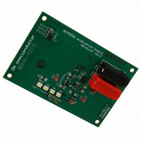
NCP5006 Figure 38. NCP5006 Demo Board PCB: Top Layer Figure 39. NCP5006 Demo Board PCB: Bottom Layer Figure 40. NCP5006 Demo Board Top Silkscreen http://onsemi.com 22 ...
Page 23
FIGURES INDEX Figure 1: Typical Application . . . . . . . . . . . . . . . . . . . . . . . . . . . . . . . . . . ...
Page 24
... H *For additional information on our Pb−Free strategy and soldering details, please download the ON Semiconductor Soldering and Mounting Techniques Reference Manual, SOLDERRM/D. ON Semiconductor and are registered trademarks of Semiconductor Components Industries, LLC (SCILLC). SCILLC reserves the right to make changes without further notice to any products herein ...