NCP5006EVB ON Semiconductor, NCP5006EVB Datasheet - Page 5
NCP5006EVB
Manufacturer Part Number
NCP5006EVB
Description
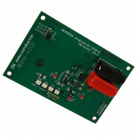
EVAL BOARD FOR NCP5006
Manufacturer
ON Semiconductor
Specifications of NCP5006EVB
Design Resources
NCP5006 Demo Board BOM NCP5006EVB Gerber Files NCP5006 Demo Board Schematic
Current - Output / Channel
15mA
Outputs And Type
1, Non-Isolated
Voltage - Output
22V
Voltage - Input
3.6V
Utilized Ic / Part
NCP5006
Core Chip
NCP5006
Topology
Boost
No. Of Outputs
1
Development Tool Type
Hardware - Eval/Demo Board
Mcu Supported Families
NCP5006
Lead Free Status / RoHS Status
Lead free / RoHS Compliant
Features
-
Lead Free Status / Rohs Status
Lead free / RoHS Compliant
For Use With/related Products
NCP5006
Other names
NCP5006EVBOS


5. The overall tolerance depends upon the accuracy of the external resistor.
ESD PROTECTION
The NCP5006 includes silicon devices to protect the pins
against the ESD spikes voltages. To cope with the different
ESD voltages developed in the applications, the built−in
structures have been designed to handle "2.0 kV
Body Model (HBM) and "200 V in Machine Model (MM)
on each pin.
DC/DC OPERATION
current to the external load, the circuit being powered from
a standard battery supply. Since the regulation is made by
ANALOG SECTION
temperature, unless otherwise noted.)
High Level Input Voltage
Low Level Input Voltage
EN Pull Down Resistor
Feedback Voltage Threshold
Output Current Stabilization Time Delay following a DC/DC Start−up,
Internal Switch ON Resistor @ Tamb = +25°C
The DC/DC converter is designed to supply a constant
@ V
CONTROL
LOGIC
bat
= 3.60 V, L = 22 mH, I
TIME_OUT
ZERO_CROSSING
RESET
POR
(Typical values are referenced to T
out
= 20 mA
Rating
+
−
Figure 3. Basic DC/DC Converter Structure
V(Ipeak)
in
Human
A
http://onsemi.com
= +25°C, Min & Max values are referenced −25°C to +85°C ambient
Vref
Vd
NCP5006
sense
−
+
5
means of a current loop, the output voltage will varies
depending upon the dynamic impedance presented by the
load.
range from a low 6.40 V (two LED in series biased with a
low current), up to 21 V, the voltage compliance the chip
can sustain continuously.
a 28 V maximum rating voltage capability, the power
device can accommodate high voltage source without any
leakage current downgrading.
Considering high intensity LED, the output voltage can
The basic DC/DC structure is depicted in Figure 3. With
Pin
C2
4
4
3
1
1
GND
Vd
QR
Symbol
I
sense
R1
outdly
R
EN
FB
DSON
EN
GND
Q1 Vds
Min
185
1.3
−
−
−
−
1
3
Typ
V
100
200
100
1.7
−
−
bat
GND
L1
22 mH
D1
Max
225
0.4
R2
xR
−
−
−
−
GND
Unit
mV
kW
Vs
ms
W
V
V
Related parts for NCP5006EVB
Image
Part Number
Description
Manufacturer
Datasheet
Request
R

Part Number:
Description:
Compact Backlight LED Boost Driver
Manufacturer:
ON Semiconductor
Datasheet:
Part Number:
Description:
ON Semiconductor [VOLTAGE REGULATOR]
Manufacturer:
ON Semiconductor
Datasheet:
Part Number:
Description:
357-036-542-201 CARDEDGE 36POS DL .156 BLK LOPRO
Manufacturer:
ON Semiconductor
Datasheet:
Part Number:
Description:
357-036-542-201 CARDEDGE 36POS DL .156 BLK LOPRO
Manufacturer:
ON Semiconductor
Datasheet:
Part Number:
Description:
357-036-542-201 CARDEDGE 36POS DL .156 BLK LOPRO
Manufacturer:
ON Semiconductor
Datasheet:
Part Number:
Description:
357-036-542-201 CARDEDGE 36POS DL .156 BLK LOPRO
Manufacturer:
ON Semiconductor
Datasheet:
Part Number:
Description:
357-036-542-201 CARDEDGE 36POS DL .156 BLK LOPRO
Manufacturer:
ON Semiconductor
Datasheet:
Part Number:
Description:
357-036-542-201 CARDEDGE 36POS DL .156 BLK LOPRO
Manufacturer:
ON Semiconductor
Datasheet:
Part Number:
Description:
357-036-542-201 CARDEDGE 36POS DL .156 BLK LOPRO
Manufacturer:
ON Semiconductor
Datasheet:
Part Number:
Description:
357-036-542-201 CARDEDGE 36POS DL .156 BLK LOPRO
Manufacturer:
ON Semiconductor
Datasheet:
Part Number:
Description:
357-036-542-201 CARDEDGE 36POS DL .156 BLK LOPRO
Manufacturer:
ON Semiconductor
Datasheet:
Part Number:
Description:
357-036-542-201 CARDEDGE 36POS DL .156 BLK LOPRO
Manufacturer:
ON Semiconductor
Datasheet:
Part Number:
Description:
Manufacturer:
ON Semiconductor
Datasheet:
Part Number:
Description:
Manufacturer:
ON Semiconductor
Datasheet: