NCP5006EVB ON Semiconductor, NCP5006EVB Datasheet - Page 6
NCP5006EVB
Manufacturer Part Number
NCP5006EVB
Description
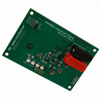
EVAL BOARD FOR NCP5006
Manufacturer
ON Semiconductor
Specifications of NCP5006EVB
Design Resources
NCP5006 Demo Board BOM NCP5006EVB Gerber Files NCP5006 Demo Board Schematic
Current - Output / Channel
15mA
Outputs And Type
1, Non-Isolated
Voltage - Output
22V
Voltage - Input
3.6V
Utilized Ic / Part
NCP5006
Core Chip
NCP5006
Topology
Boost
No. Of Outputs
1
Development Tool Type
Hardware - Eval/Demo Board
Mcu Supported Families
NCP5006
Lead Free Status / RoHS Status
Lead free / RoHS Compliant
Features
-
Lead Free Status / Rohs Status
Lead free / RoHS Compliant
For Use With/related Products
NCP5006
Other names
NCP5006EVBOS


Basically, the chip operates with two cycles:
place. When the current hits the peak value, defined by the
inductor is bounded by two limits:
•
•
Figure 4 and t
equations. (Note: The equations are for theoretical analysis
only, they do not include the losses.)
Let V
(assuming a typical V
be sized to cope with the peak current present in the circuit
The POR signal sets the flip−flop and the first cycle takes
Based on the data sheet, the current flowing into the
The system operates in a continuous mode as depicted in
Since t
Of course, from a practical stand point, the inductor must
Cycle #1: time t1, the energy is stored into the inductor
Cycle #2: time t2, the energy is dumped to the load
Ipeak Value: Internally fixed to 350 mA typical
Iv Value: Limited by the fixed Toff time built in the
chip (320 ns typical)
bat
= E, then:
2
DImax +
= 320 ns typical and Vo = 21 V maximum, then
1
and t
DI +
320 ns * (21−3.0)
t1 +
t2 +
bat
2
L + E * dI
t2 * (Vo * V bat)
times can be derived from basic
= 3.0 V):
22 mH
(Ip * Iv) * L
(Ip * Iv) * L
Vo * V bat
V bat
L
0 mA
0 mA
0 mA
dt
Ids
Io
I
L
+ 261 mA
First Start−Up
Figure 4. Basic DC−DC Operation
(eq. 1)
(eq. 2)
(eq. 3)
(eq. 4)
http://onsemi.com
NCP5006
6
Normal Operation
t1
error amplifier associated to the loop regulation, the
flip−flop resets, the NMOS is deactivated and the current
is dumped into the load. Since the timings depend on the
environment, the internal timer limits the toff cycle to
320 ns (typical), making sure the system operates in a
continuous mode to maximize the energy transfer.
to avoid saturation of the core. On top of that, the ferrite
material shall be capable to operate at high frequency
(1.0 MHz) to minimize the Foucault’s losses developed
during the cycles.
electrical parameters. Let V = Vo − V
Equation 1:
typical time), the dI is constant for a given load and
inductance value. Rearranging Equation 5 yields:
one watt: Figure 5 shows the maximum power that can be
delivered by the chip as a function of the output voltage.
The operating frequency can be derived from the
Since toff is nearly constant (according to the 320 ns
Let E = V
Finally, the operating frequency is:
The output power supplied by the NCP5006 is limited to
t2
bat
, and Vopk = output peak voltage, then:
ton +
f +
t
t
t
ton ) toff
Ipeak
Iv
ton +
ton + dI * L
(Vopk * V bat ) * dt
1
V*dt
V bat
L
E
E
* L
bat
, rearranging
(eq. 5)
(eq. 6)
(eq. 7)
(eq. 8)
Related parts for NCP5006EVB
Image
Part Number
Description
Manufacturer
Datasheet
Request
R

Part Number:
Description:
Compact Backlight LED Boost Driver
Manufacturer:
ON Semiconductor
Datasheet:
Part Number:
Description:
ON Semiconductor [VOLTAGE REGULATOR]
Manufacturer:
ON Semiconductor
Datasheet:
Part Number:
Description:
357-036-542-201 CARDEDGE 36POS DL .156 BLK LOPRO
Manufacturer:
ON Semiconductor
Datasheet:
Part Number:
Description:
357-036-542-201 CARDEDGE 36POS DL .156 BLK LOPRO
Manufacturer:
ON Semiconductor
Datasheet:
Part Number:
Description:
357-036-542-201 CARDEDGE 36POS DL .156 BLK LOPRO
Manufacturer:
ON Semiconductor
Datasheet:
Part Number:
Description:
357-036-542-201 CARDEDGE 36POS DL .156 BLK LOPRO
Manufacturer:
ON Semiconductor
Datasheet:
Part Number:
Description:
357-036-542-201 CARDEDGE 36POS DL .156 BLK LOPRO
Manufacturer:
ON Semiconductor
Datasheet:
Part Number:
Description:
357-036-542-201 CARDEDGE 36POS DL .156 BLK LOPRO
Manufacturer:
ON Semiconductor
Datasheet:
Part Number:
Description:
357-036-542-201 CARDEDGE 36POS DL .156 BLK LOPRO
Manufacturer:
ON Semiconductor
Datasheet:
Part Number:
Description:
357-036-542-201 CARDEDGE 36POS DL .156 BLK LOPRO
Manufacturer:
ON Semiconductor
Datasheet:
Part Number:
Description:
357-036-542-201 CARDEDGE 36POS DL .156 BLK LOPRO
Manufacturer:
ON Semiconductor
Datasheet:
Part Number:
Description:
357-036-542-201 CARDEDGE 36POS DL .156 BLK LOPRO
Manufacturer:
ON Semiconductor
Datasheet:
Part Number:
Description:
Manufacturer:
ON Semiconductor
Datasheet:
Part Number:
Description:
Manufacturer:
ON Semiconductor
Datasheet: