NCP5005GEVB ON Semiconductor, NCP5005GEVB Datasheet - Page 16
NCP5005GEVB
Manufacturer Part Number
NCP5005GEVB
Description
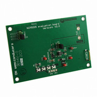
EVAL BOARD FOR NCP5005G
Manufacturer
ON Semiconductor
Specifications of NCP5005GEVB
Design Resources
NCP5005 EVB BOM NCP5005GEVB Gerber Files NCP5005 EVB Schematic
Outputs And Type
1, Non-Isolated
Voltage - Output
22V
Voltage - Input
3.6V
Utilized Ic / Part
NCP5005
Core Chip
NCP5005
Topology
Boost
No. Of Outputs
1
Development Tool Type
Hardware - Eval/Demo Board
Leaded Process Compatible
Yes
Mcu Supported Families
NCP5005SNT1G
Rohs Compliant
Yes
Lead Free Status / RoHS Status
Lead free / RoHS Compliant
Features
-
Current - Output / Channel
-
Lead Free Status / Rohs Status
Lead free / RoHS Compliant
For Use With/related Products
NCP5005G
Other names
NCP5005GEVBOS


input as an operational amplifier with a high impedance
input (reference schematic Figure 29). The analog loop
will keep going to balance the current flowing through the
sense resistor R1 until the feedback voltage is 200 mV. An
extra resistor (R4) isolates the FB node from low resistance
to ground, making possible to add an external voltage to
this pin.
added to the node Pin 1, while R2/R3/R4/R1/C3 create the
discharge time constant. In order to minimize the pick up
noise at FB node, the resistors shall have relative medium
NOTE: RC filter R2 and C3 is optional (see text)
To implement such a function, let consider the feedback
The time constant R2/C3 generates the voltage across C3,
PWM
Average Network
150 k
R2
Figure 29. Basic DC Current Mode Operation with PWM Control
Figure 30. Operation with Analog PWM, f = 10 kHz, DC = 25%
GND
GND
C3
100 nF
10 k
R3
10 W
R1
GND
http://onsemi.com
5.6 k
R4
V
NCP5005
bat
Sense Resistor
LWT67C LWT67C LWT67C LWT67C LWT67C
16
4
2
3
D6
NCP5005
U1
EN
GND
FB
value, preferably well below 1.0 MW. Consequently, let R2 =
150 k, R3 = 10 k and R4 = 5.6 k. On the other hand, the
feedback delay to control the luminosity of the LED shall be
acceptable by the user, 10 ms or less being a good
compromise. The time constant can now be calculated based
on a 400 mV offset voltage at the C3/R2/R3 node to force
zero current to the LED. Assuming the PWM signal comes
from a standard gate powered by a 3.0 V supply, running at
10 kHz, then a full dimming of the LED can be achieved with
a 95% span of the Duty Cycle signal. Figure 30 depicts the
behavior under such PWM analog mode.
D5
V
V
bat
out
5
1
V
D4
bat
L1
22 mH
D3
MBR0530
D1
PWM
VPWM
4.7 mF
VFB
C1
D2
GND
GND
C2
1.0 mF
Related parts for NCP5005GEVB
Image
Part Number
Description
Manufacturer
Datasheet
Request
R

Part Number:
Description:
Compact Backlight LED Boost Driver
Manufacturer:
ON Semiconductor
Datasheet:
Part Number:
Description:
ON Semiconductor [VOLTAGE REGULATOR]
Manufacturer:
ON Semiconductor
Datasheet:
Part Number:
Description:
357-036-542-201 CARDEDGE 36POS DL .156 BLK LOPRO
Manufacturer:
ON Semiconductor
Datasheet:
Part Number:
Description:
357-036-542-201 CARDEDGE 36POS DL .156 BLK LOPRO
Manufacturer:
ON Semiconductor
Datasheet:
Part Number:
Description:
357-036-542-201 CARDEDGE 36POS DL .156 BLK LOPRO
Manufacturer:
ON Semiconductor
Datasheet:
Part Number:
Description:
357-036-542-201 CARDEDGE 36POS DL .156 BLK LOPRO
Manufacturer:
ON Semiconductor
Datasheet:
Part Number:
Description:
357-036-542-201 CARDEDGE 36POS DL .156 BLK LOPRO
Manufacturer:
ON Semiconductor
Datasheet:
Part Number:
Description:
357-036-542-201 CARDEDGE 36POS DL .156 BLK LOPRO
Manufacturer:
ON Semiconductor
Datasheet:
Part Number:
Description:
357-036-542-201 CARDEDGE 36POS DL .156 BLK LOPRO
Manufacturer:
ON Semiconductor
Datasheet:
Part Number:
Description:
357-036-542-201 CARDEDGE 36POS DL .156 BLK LOPRO
Manufacturer:
ON Semiconductor
Datasheet:
Part Number:
Description:
357-036-542-201 CARDEDGE 36POS DL .156 BLK LOPRO
Manufacturer:
ON Semiconductor
Datasheet:
Part Number:
Description:
357-036-542-201 CARDEDGE 36POS DL .156 BLK LOPRO
Manufacturer:
ON Semiconductor
Datasheet:
Part Number:
Description:
Manufacturer:
ON Semiconductor
Datasheet:
Part Number:
Description:
Manufacturer:
ON Semiconductor
Datasheet: