NCP5005GEVB ON Semiconductor, NCP5005GEVB Datasheet - Page 4
NCP5005GEVB
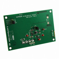
Manufacturer Part Number
NCP5005GEVB
Description
EVAL BOARD FOR NCP5005G
Manufacturer
ON Semiconductor
Specifications of NCP5005GEVB
Design Resources
NCP5005 EVB BOM NCP5005GEVB Gerber Files NCP5005 EVB Schematic
Outputs And Type
1, Non-Isolated
Voltage - Output
22V
Voltage - Input
3.6V
Utilized Ic / Part
NCP5005
Core Chip
NCP5005
Topology
Boost
No. Of Outputs
1
Development Tool Type
Hardware - Eval/Demo Board
Leaded Process Compatible
Yes
Mcu Supported Families
NCP5005SNT1G
Rohs Compliant
Yes
Lead Free Status / RoHS Status
Lead free / RoHS Compliant
Features
-
Current - Output / Channel
-
Lead Free Status / Rohs Status
Lead free / RoHS Compliant
For Use With/related Products
NCP5005G
Other names
NCP5005GEVBOS


Maximum ratings are those values beyond which device damage can occur. Maximum ratings applied to the device are individual stress limit values
(not normal operating conditions) and are not valid simultaneously. If these limits are exceeded, device functional operation is not implied, damage
may occur and reliability may be affected.
1. This device series contains ESD protection and exceeds the following tests:
2. The maximum package power dissipation limit must not be exceeded.
3. Latch−up current maximum rating: "100 mA per JEDEC standard: JESD78.
4. Moisture Sensivity Level (MSL): 1 per IPC/JEDEC standard: J−STD−020A.
MAXIMUM RATINGS
POWER SUPPLY SECTION
temperature, unless otherwise noted.)
Power Supply
Output Power Supply Voltage Compliance
Digital Input Voltage
Digital Input Current
ESD Capability (Note 1)
TSOP−5 Package
Operating Ambient Temperature Range
Operating Junction Temperature Range
Maximum Junction Temperature
Storage Temperature Range
Power Supply
Output Load Voltage Compliance
Continuous DC Current in the Load @ V
Stand By Current, @ I
Stand By Current, @ I
Inductor Discharging Time @ V
Thermal Shutdown Protection
Thermal Shutdown Protection Hysteresis
Human Body Model (HBM)
Machine Model (MM)
Power Dissipation @ T
Thermal Resistance, Junction−to−Air
ESR < 1.5 W, V
I
out
Human Body Model (HBM) "2.0 kV per JEDEC standard: JESD22−A114
Machine Model (MM) "200 V per JEDEC standard: JESD22−A115
= 10 mA
bat
= 3.60 V
out
out
A
= 0 mA, EN = L, V
= 0 mA, EN = L, V
= +85°C (Note 2)
bat
(Typical values are referenced to T
Rating
Rating
= 3.6 V, L = 22 mH, 3xLED,
out
= 3xLED, L = 22 mH,
bat
bat
= 3.6 V
= 5.5 V
http://onsemi.com
NCP5005
A
4
= +25°C, Min & Max values are referenced −25°C to +85°C ambient
Pin
4
5
5
4
4
4
−
−
Symbol
T
V
R
V
V
T
EN
Jmax
P
T
ESD
T
qJA
bat
out
stg
D
A
J
Symbol
Toffmax
T
V
V
I
I
T
I
stdb
stdb
SDH
out
bat
out
SD
−0.3 < V
Min
−25 to +125
−65 to +150
2.7
21
50
−25 to +85
−
−
−
−
−
Value
in
+150
200
160
250
6.0
1.0
2.0
28
< V
bat
Typ
320
160
0.3
0.8
24
30
−
−
+ 0.3
Max
5.5
3.0
−
−
−
−
−
−
°C/W
Unit
mW
mA
kV
°C
°C
°C
°C
V
V
V
V
Unit
mA
mA
mA
ns
°C
°C
V
V
Related parts for NCP5005GEVB
Image
Part Number
Description
Manufacturer
Datasheet
Request
R

Part Number:
Description:
Compact Backlight LED Boost Driver
Manufacturer:
ON Semiconductor
Datasheet:
Part Number:
Description:
ON Semiconductor [VOLTAGE REGULATOR]
Manufacturer:
ON Semiconductor
Datasheet:
Part Number:
Description:
357-036-542-201 CARDEDGE 36POS DL .156 BLK LOPRO
Manufacturer:
ON Semiconductor
Datasheet:
Part Number:
Description:
357-036-542-201 CARDEDGE 36POS DL .156 BLK LOPRO
Manufacturer:
ON Semiconductor
Datasheet:
Part Number:
Description:
357-036-542-201 CARDEDGE 36POS DL .156 BLK LOPRO
Manufacturer:
ON Semiconductor
Datasheet:
Part Number:
Description:
357-036-542-201 CARDEDGE 36POS DL .156 BLK LOPRO
Manufacturer:
ON Semiconductor
Datasheet:
Part Number:
Description:
357-036-542-201 CARDEDGE 36POS DL .156 BLK LOPRO
Manufacturer:
ON Semiconductor
Datasheet:
Part Number:
Description:
357-036-542-201 CARDEDGE 36POS DL .156 BLK LOPRO
Manufacturer:
ON Semiconductor
Datasheet:
Part Number:
Description:
357-036-542-201 CARDEDGE 36POS DL .156 BLK LOPRO
Manufacturer:
ON Semiconductor
Datasheet:
Part Number:
Description:
357-036-542-201 CARDEDGE 36POS DL .156 BLK LOPRO
Manufacturer:
ON Semiconductor
Datasheet:
Part Number:
Description:
357-036-542-201 CARDEDGE 36POS DL .156 BLK LOPRO
Manufacturer:
ON Semiconductor
Datasheet:
Part Number:
Description:
357-036-542-201 CARDEDGE 36POS DL .156 BLK LOPRO
Manufacturer:
ON Semiconductor
Datasheet:
Part Number:
Description:
Manufacturer:
ON Semiconductor
Datasheet:
Part Number:
Description:
Manufacturer:
ON Semiconductor
Datasheet: