NCP5005GEVB ON Semiconductor, NCP5005GEVB Datasheet - Page 17
NCP5005GEVB
Manufacturer Part Number
NCP5005GEVB
Description
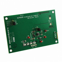
EVAL BOARD FOR NCP5005G
Manufacturer
ON Semiconductor
Specifications of NCP5005GEVB
Design Resources
NCP5005 EVB BOM NCP5005GEVB Gerber Files NCP5005 EVB Schematic
Outputs And Type
1, Non-Isolated
Voltage - Output
22V
Voltage - Input
3.6V
Utilized Ic / Part
NCP5005
Core Chip
NCP5005
Topology
Boost
No. Of Outputs
1
Development Tool Type
Hardware - Eval/Demo Board
Leaded Process Compatible
Yes
Mcu Supported Families
NCP5005SNT1G
Rohs Compliant
Yes
Lead Free Status / RoHS Status
Lead free / RoHS Compliant
Features
-
Current - Output / Channel
-
Lead Free Status / Rohs Status
Lead free / RoHS Compliant
For Use With/related Products
NCP5005G
Other names
NCP5005GEVBOS


Digital Control
be implemented by providing a PWM signal to this pin (see
Figure 31). The output current depends upon the Duty
control, is depicted in Figures 32 and 33. The tests have
Due to the EN pin, a digitally controlled luminosity can
The PWM operation, using the EN pin as a digital
Pulse
GND
NOTE: Pulse width and frequency depends upon the application constraints.
Figure 31. Typical Semi−Pulsed Mode of Operation
22 W
Figure 32. Operation @ PWM = 10 kHz, DC = 10%
R1
GND
LWT67C LWT67C LWT67C LWT67C LWT67C
4
2
3
D6
NCP5005
U1
EN
GND
FB
http://onsemi.com
NCP5005
D5
V
V
out
bat
17
5
1
Cycle, but care must be observed as the DC/DC converter
is continuously pulsed ON/OFF and noise are likely to be
generated.
been carried out at room temperature with V
L = 22 mH, five LEDs in series, RFB = 22 W.
V
D4
bat
L1
22 mH
D3
MBR0530
D1
4.7 mF
C1
D2
GND
V
load
GND
VPWM
VFB
V
C2
1.0 mF
PWM
load
bat
= 3.60 V,
Related parts for NCP5005GEVB
Image
Part Number
Description
Manufacturer
Datasheet
Request
R

Part Number:
Description:
Compact Backlight LED Boost Driver
Manufacturer:
ON Semiconductor
Datasheet:
Part Number:
Description:
ON Semiconductor [VOLTAGE REGULATOR]
Manufacturer:
ON Semiconductor
Datasheet:
Part Number:
Description:
357-036-542-201 CARDEDGE 36POS DL .156 BLK LOPRO
Manufacturer:
ON Semiconductor
Datasheet:
Part Number:
Description:
357-036-542-201 CARDEDGE 36POS DL .156 BLK LOPRO
Manufacturer:
ON Semiconductor
Datasheet:
Part Number:
Description:
357-036-542-201 CARDEDGE 36POS DL .156 BLK LOPRO
Manufacturer:
ON Semiconductor
Datasheet:
Part Number:
Description:
357-036-542-201 CARDEDGE 36POS DL .156 BLK LOPRO
Manufacturer:
ON Semiconductor
Datasheet:
Part Number:
Description:
357-036-542-201 CARDEDGE 36POS DL .156 BLK LOPRO
Manufacturer:
ON Semiconductor
Datasheet:
Part Number:
Description:
357-036-542-201 CARDEDGE 36POS DL .156 BLK LOPRO
Manufacturer:
ON Semiconductor
Datasheet:
Part Number:
Description:
357-036-542-201 CARDEDGE 36POS DL .156 BLK LOPRO
Manufacturer:
ON Semiconductor
Datasheet:
Part Number:
Description:
357-036-542-201 CARDEDGE 36POS DL .156 BLK LOPRO
Manufacturer:
ON Semiconductor
Datasheet:
Part Number:
Description:
357-036-542-201 CARDEDGE 36POS DL .156 BLK LOPRO
Manufacturer:
ON Semiconductor
Datasheet:
Part Number:
Description:
357-036-542-201 CARDEDGE 36POS DL .156 BLK LOPRO
Manufacturer:
ON Semiconductor
Datasheet:
Part Number:
Description:
Manufacturer:
ON Semiconductor
Datasheet:
Part Number:
Description:
Manufacturer:
ON Semiconductor
Datasheet: