DK-35TS-LPC2478 Future Designs Inc, DK-35TS-LPC2478 Datasheet - Page 10
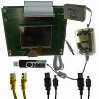
DK-35TS-LPC2478
Manufacturer Part Number
DK-35TS-LPC2478
Description
PROGRAMMERS, DEVELOPMENT SYSTEMS
Manufacturer
Future Designs Inc
Specifications of DK-35TS-LPC2478
Sensor Type
Touch Screen
Interface
I²C
Voltage - Supply
5V
Embedded
Yes, MCU, 16/32-Bit
Utilized Ic / Part
LPC2478 ARM7
For Use With
568-4742 - MODULE DIMM LPC2478 ARM7
Lead Free Status / RoHS Status
Lead free / RoHS Compliant
Sensitivity
-
Sensing Range
-
Other names
622-1034
ARM-35TS-LPC2478
ARM-35TS-LPC2478


NXP Semiconductors
Table 4.
LPC2478
Product data sheet
Symbol
P0[0] to P0[31]
P0[0]/RD1/TXD3/
SDA1
P0[1]/TD1/RXD3/
SCL1
P0[2]/TXD0
P0[3]/RXD0
P0[4]/I2SRX_CLK/
LCDVD[0]/RD2/
CAP2[0]
P0[5]/I2SRX_WS/
LCDVD[1]/TD2/
CAP2[1]
P0[6]/I2SRX_SDA/
LCDVD[8]/
SSEL1/MAT2[0]
Pin description
6.2 Pin description
Pin
94
96
202
204
168
166
164
[1]
[1]
[1]
[1]
[1]
[1]
[1]
Ball
U15
T14
C4
D6
B12
C12
D13
[1]
[1]
[1]
[1]
[1]
[1]
[1]
All information provided in this document is subject to legal disclaimers.
Type
I/O
I/O
I
O
I/O
I/O
O
I
I/O
I/O
O
I/O
I
I/O
I/O
O
I
I
I/O
I/O
O
O
I
I/O
I/O
O
I/O
O
Rev. 2 — 29 September 2010
Description
Port 0: Port 0 is a 32-bit I/O port with individual direction controls for each
bit. The operation of port 0 pins depends upon the pin function selected
via the pin connect block.
P0[0] — General purpose digital input/output pin.
RD1 — CAN1 receiver input.
TXD3 — Transmitter output for UART3.
SDA1 — I
P0[1] — General purpose digital input/output pin.
TD1 — CAN1 transmitter output.
RXD3 — Receiver input for UART3.
SCL1 — I
P0[2] — General purpose digital input/output pin.
TXD0 — Transmitter output for UART0.
P0[3] — General purpose digital input/output pin.
RXD0 — Receiver input for UART0.
P0[4] — General purpose digital input/output pin.
I2SRX_CLK — I
by the slave. Corresponds to the signal SCK in the I2S-bus
specification.
LCDVD[0] — LCD data.
RD2 — CAN2 receiver input.
CAP2[0] — Capture input for Timer 2, channel 0.
P0[5] — General purpose digital input/output pin.
I2SRX_WS — I
received by the slave. Corresponds to the signal WS in the I
specification.
LCDVD[1] — LCD data.
TD2 — CAN2 transmitter output.
CAP2[1] — Capture input for Timer 2, channel 1.
P0[6] — General purpose digital input/output pin.
I2SRX_SDA — I
by the receiver. Corresponds to the signal SD in the I
specification.
LCDVD[8] — LCD data.
SSEL1 — Slave Select for SSP1.
MAT2[0] — Match output for Timer 2, channel 0.
2
2
C1 clock input/output (this is not an open-drain pin).
C1 data input/output (this is not an open-drain pin).
[17]
[17]
[17]
2
2
S Receive word select. It is driven by the master and
2
S Receive clock. It is driven by the master and received
S Receive data. It is driven by the transmitter and read
[17]
[17]
[17]
Single-chip 16-bit/32-bit microcontroller
LPC2478
2
© NXP B.V. 2010. All rights reserved.
S-bus
2
S-bus
10 of 91
Related parts for DK-35TS-LPC2478
Image
Part Number
Description
Manufacturer
Datasheet
Request
R

Part Number:
Description:
SOCKET ADAPTER BOARD
Manufacturer:
Future Designs Inc
Datasheet:

Part Number:
Description:
BOARD SCKT ADAPTER FOR TFBGA100
Manufacturer:
Future Designs Inc

Part Number:
Description:
BOARD SCKT ADAPTER FOR TFBGA180
Manufacturer:
Future Designs Inc

Part Number:
Description:
BOARD SCKT ADAPTER FOR TFBGA208
Manufacturer:
Future Designs Inc


Part Number:
Description:
BOARD DEMO FOR PHILIPS PCA9633
Manufacturer:
Future Designs Inc
Datasheet:

Part Number:
Description:
KIT LCD TOUCH 5.7" FOR LPC2478
Manufacturer:
Future Designs Inc

Part Number:
Description:
KIT LCD TOUCH 5.7" FOR LPC3250
Manufacturer:
Future Designs Inc

Part Number:
Description:
BOARD FOR LPC2103 48-LQFP
Manufacturer:
Future Designs Inc


Part Number:
Description:
KIT DEV IND REF DESIGN LPC1768
Manufacturer:
Future Designs Inc

Part Number:
Description:
BOARD FOR LPC9103 10-HVSON
Manufacturer:
Future Designs Inc
