DK-35TS-LPC2478 Future Designs Inc, DK-35TS-LPC2478 Datasheet - Page 27
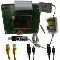
DK-35TS-LPC2478
Manufacturer Part Number
DK-35TS-LPC2478
Description
PROGRAMMERS, DEVELOPMENT SYSTEMS
Manufacturer
Future Designs Inc
Specifications of DK-35TS-LPC2478
Sensor Type
Touch Screen
Interface
I²C
Voltage - Supply
5V
Embedded
Yes, MCU, 16/32-Bit
Utilized Ic / Part
LPC2478 ARM7
For Use With
568-4742 - MODULE DIMM LPC2478 ARM7
Lead Free Status / RoHS Status
Lead free / RoHS Compliant
Sensitivity
-
Sensing Range
-
Other names
622-1034
ARM-35TS-LPC2478
ARM-35TS-LPC2478


NXP Semiconductors
7. Functional description
LPC2478
Product data sheet
7.1 Architectural overview
The LPC2478 microcontroller consists of an ARM7TDMI-S CPU with emulation support,
the ARM7 local bus for closely coupled, high-speed access to the majority of on-chip
memory, the AMBA AHB interfacing to high-speed on-chip peripherals and external
memory, and the AMBA APB for connection to other on-chip peripheral functions. The
microcontroller permanently configures the ARM7TDMI-S processor for little-endian byte
order.
The LPC2478 implements two AHBs in order to allow the Ethernet block to operate
without interference caused by other system activity. The primary AHB, referred to as
AHB1, includes the VIC, GPDMA controller, and EMC.
The second AHB, referred to as AHB2, includes only the Ethernet block and an
associated 16 kB SRAM. In addition, a bus bridge is provided that allows the secondary
AHB to be a bus master on AHB1, allowing expansion of Ethernet buffer space into
off-chip memory or unused space in memory residing on AHB1.
In summary, bus masters with access to AHB1 are the ARM7 itself, the GPDMA function,
and the Ethernet block (via the bus bridge from AHB2). Bus masters with access to AHB2
are the ARM7 and the Ethernet block.
AHB peripherals are allocated a 2 MB range of addresses at the very top of the 4 GB
ARM memory space. Each AHB peripheral is allocated a 16 kB address space within the
AHB address space. Lower speed peripheral functions are connected to the APB. The
AHB to APB bridge interfaces the APB to the AHB. APB peripherals are also allocated a
2 MB range of addresses, beginning at the 3.5 GB address point. Each APB peripheral is
allocated a 16 kB address space within the APB address space.
The ARM7TDMI-S processor is a general purpose 32-bit microprocessor, which offers
high performance and very low power consumption. The ARM architecture is based on
Reduced Instruction Set Computer (RISC) principles, and the instruction set and related
decode mechanism are much simpler than those of microprogrammed complex
instruction set computers. This simplicity results in a high instruction throughput and
impressive real-time interrupt response from a small and cost-effective processor core.
Pipeline techniques are employed so that all parts of the processing and memory systems
can operate continuously. Typically, while one instruction is being executed, its successor
is being decoded, and a third instruction is being fetched from memory.
The ARM7TDMI-S processor also employs a unique architectural strategy known as
Thumb, which makes it ideally suited to high-volume applications with memory
restrictions, or applications where code density is an issue.
The key idea behind Thumb is that of a super-reduced instruction set. Essentially, the
ARM7TDMI-S processor has two instruction sets:
•
•
the standard 32-bit ARM set
a 16-bit Thumb set
All information provided in this document is subject to legal disclaimers.
Rev. 2 — 29 September 2010
Single-chip 16-bit/32-bit microcontroller
LPC2478
© NXP B.V. 2010. All rights reserved.
27 of 91
Related parts for DK-35TS-LPC2478
Image
Part Number
Description
Manufacturer
Datasheet
Request
R

Part Number:
Description:
SOCKET ADAPTER BOARD
Manufacturer:
Future Designs Inc
Datasheet:

Part Number:
Description:
BOARD SCKT ADAPTER FOR TFBGA100
Manufacturer:
Future Designs Inc

Part Number:
Description:
BOARD SCKT ADAPTER FOR TFBGA180
Manufacturer:
Future Designs Inc

Part Number:
Description:
BOARD SCKT ADAPTER FOR TFBGA208
Manufacturer:
Future Designs Inc


Part Number:
Description:
BOARD DEMO FOR PHILIPS PCA9633
Manufacturer:
Future Designs Inc
Datasheet:

Part Number:
Description:
KIT LCD TOUCH 5.7" FOR LPC2478
Manufacturer:
Future Designs Inc

Part Number:
Description:
KIT LCD TOUCH 5.7" FOR LPC3250
Manufacturer:
Future Designs Inc

Part Number:
Description:
BOARD FOR LPC2103 48-LQFP
Manufacturer:
Future Designs Inc


Part Number:
Description:
KIT DEV IND REF DESIGN LPC1768
Manufacturer:
Future Designs Inc

Part Number:
Description:
BOARD FOR LPC9103 10-HVSON
Manufacturer:
Future Designs Inc
