DK-35TS-LPC2478 Future Designs Inc, DK-35TS-LPC2478 Datasheet - Page 47
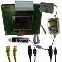
DK-35TS-LPC2478
Manufacturer Part Number
DK-35TS-LPC2478
Description
PROGRAMMERS, DEVELOPMENT SYSTEMS
Manufacturer
Future Designs Inc
Specifications of DK-35TS-LPC2478
Sensor Type
Touch Screen
Interface
I²C
Voltage - Supply
5V
Embedded
Yes, MCU, 16/32-Bit
Utilized Ic / Part
LPC2478 ARM7
For Use With
568-4742 - MODULE DIMM LPC2478 ARM7
Lead Free Status / RoHS Status
Lead free / RoHS Compliant
Sensitivity
-
Sensing Range
-
Other names
622-1034
ARM-35TS-LPC2478
ARM-35TS-LPC2478


NXP Semiconductors
LPC2478
Product data sheet
7.26.4.4 Deep power-down mode
7.26.4.5 Power domains
the meantime, the flash wake-up timer then counts 4 MHz IRC clock cycles to make the
100 μs flash start-up time. When it times out, access to the flash will be allowed. The
customers need to reconfigure the PLL and clock dividers accordingly.
Deep power-down mode is similar to the Power-down mode, but now the on-chip
regulator that supplies power to the internal logic is also shut off. This produces the lowest
possible power consumption without removing power from the entire chip. Since the Deep
power-down mode shuts down the on-chip logic power supply, there is no register or
memory retention, and resumption of operation involves the same activities as a full chip
reset.
If power is supplied to the LPC2478 during Deep power-down mode, wake-up can be
caused by the RTC Alarm interrupt or by external Reset.
While in Deep power-down mode, external device power may be removed. In this case,
the LPC2478 will start up when external power is restored.
Essential data may be retained through Deep power-down mode (or through complete
powering off of the chip) by storing data in the Battery RAM, as long as the external power
to the VBAT pin is maintained.
The LPC2478 provides two independent power domains that allow the bulk of the device
to have power removed while maintaining operation of the RTC and the Battery RAM.
On the LPC2478, I/O pads are powered by the 3.3 V (V
V
the CPU and most of the peripherals.
Although both the I/O pad ring and the core require a 3.3 V supply, different powering
schemes can be used depending on the actual application requirements.
The first option assumes that power consumption is not a concern and the design ties the
V
supply for both pads, the CPU, and peripherals. While this solution is simple, it does not
support powering down the I/O pad ring “on the fly” while keeping the CPU and
peripherals alive.
The second option uses two power supplies; a 3.3 V supply for the I/O pads (V
a dedicated 3.3 V supply for the CPU (V
converter powered independently from the I/O pad ring enables shutting down of the I/O
pad power supply “on the fly”, while the CPU and peripherals stay active.
The VBAT pin supplies power only to the RTC and the Battery RAM. These two functions
require a minimum of power to operate, which can be supplied by an external battery.
When the CPU and the rest of chip functions are stopped and power removed, the RTC
can supply an alarm output that may be used by external hardware to restore chip power
and resume operation.
DD(DCDC)(3V3)
DD(3V3)
and V
pins power the on-chip DC-to-DC converter which in turn provides power to
DD(DCDC)(3V3)
All information provided in this document is subject to legal disclaimers.
Rev. 2 — 29 September 2010
pins together. This approach requires only one 3.3 V power
DD(DCDC)(3V3)
Single-chip 16-bit/32-bit microcontroller
). Having the on-chip DC-DC
DD(3V3)
) pins, while the
LPC2478
© NXP B.V. 2010. All rights reserved.
DD(3V3)
47 of 91
) and
Related parts for DK-35TS-LPC2478
Image
Part Number
Description
Manufacturer
Datasheet
Request
R

Part Number:
Description:
SOCKET ADAPTER BOARD
Manufacturer:
Future Designs Inc
Datasheet:

Part Number:
Description:
BOARD SCKT ADAPTER FOR TFBGA100
Manufacturer:
Future Designs Inc

Part Number:
Description:
BOARD SCKT ADAPTER FOR TFBGA180
Manufacturer:
Future Designs Inc

Part Number:
Description:
BOARD SCKT ADAPTER FOR TFBGA208
Manufacturer:
Future Designs Inc


Part Number:
Description:
BOARD DEMO FOR PHILIPS PCA9633
Manufacturer:
Future Designs Inc
Datasheet:

Part Number:
Description:
KIT LCD TOUCH 5.7" FOR LPC2478
Manufacturer:
Future Designs Inc

Part Number:
Description:
KIT LCD TOUCH 5.7" FOR LPC3250
Manufacturer:
Future Designs Inc

Part Number:
Description:
BOARD FOR LPC2103 48-LQFP
Manufacturer:
Future Designs Inc


Part Number:
Description:
KIT DEV IND REF DESIGN LPC1768
Manufacturer:
Future Designs Inc

Part Number:
Description:
BOARD FOR LPC9103 10-HVSON
Manufacturer:
Future Designs Inc
