DK-35TS-LPC2478 Future Designs Inc, DK-35TS-LPC2478 Datasheet - Page 48
DK-35TS-LPC2478
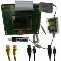
Manufacturer Part Number
DK-35TS-LPC2478
Description
PROGRAMMERS, DEVELOPMENT SYSTEMS
Manufacturer
Future Designs Inc
Specifications of DK-35TS-LPC2478
Sensor Type
Touch Screen
Interface
I²C
Voltage - Supply
5V
Embedded
Yes, MCU, 16/32-Bit
Utilized Ic / Part
LPC2478 ARM7
For Use With
568-4742 - MODULE DIMM LPC2478 ARM7
Lead Free Status / RoHS Status
Lead free / RoHS Compliant
Sensitivity
-
Sensing Range
-
Other names
622-1034
ARM-35TS-LPC2478
ARM-35TS-LPC2478


NXP Semiconductors
LPC2478
Product data sheet
7.27.1 Reset
7.27.2 Brownout detection
7.27.3 Code security (Code Read Protection - CRP)
7.27 System control
Reset has four sources on the LPC2478: the RESET pin, the Watchdog reset, power-on
reset, and the BrownOut Detection (BOD) circuit. The RESET pin is a Schmitt trigger input
pin. Assertion of chip Reset by any source, once the operating voltage attains a usable
level, starts the wake-up timer (see description in
causing reset to remain asserted until the external Reset is de-asserted, the oscillator is
running, a fixed number of clocks have passed, and the flash controller has completed its
initialization.
When the internal Reset is removed, the processor begins executing at address 0, which
is initially the Reset vector mapped from the Boot Block. At that point, all of the processor
and peripheral registers have been initialized to predetermined values.
The LPC2478 includes 2-stage monitoring of the voltage on the V
voltage falls below 2.95 V, the BOD asserts an interrupt signal to the Vectored Interrupt
Controller. This signal can be enabled for interrupt in the Interrupt Enable Register in the
VIC in order to cause a CPU interrupt; if not, software can monitor the signal by reading a
dedicated status register.
The second stage of low-voltage detection asserts Reset to inactivate the LPC2478 when
the voltage on the V
the flash as operation of the various elements of the chip would otherwise become
unreliable due to low voltage. The BOD circuit maintains this reset down below 1 V, at
which point the power-on reset circuitry maintains the overall Reset.
Both the 2.95 V and 2.65 V thresholds include some hysteresis. In normal operation, this
hysteresis allows the 2.95 V detection to reliably interrupt, or a regularly-executed event
loop to sense the condition.
This feature of the LPC2478 allows user to enable different levels of security in the system
so that access to the on-chip flash and use of the JTAG and ISP can be restricted. When
needed, CRP is invoked by programming a specific pattern into a dedicated flash location.
IAP commands are not affected by the CRP.
There are three levels of the Code Read Protection.
CRP1 disables access to chip via the JTAG and allows partial flash update (excluding
flash sector 0) using a limited set of the ISP commands. This mode is useful when CRP is
required and flash field updates are needed but all sectors can not be erased.
CRP2 disables access to chip via the JTAG and only allows full flash erase and update
using a reduced set of the ISP commands.
Running an application with level CRP3 selected fully disables any access to chip via the
JTAG pins and the ISP. This mode effectively disables ISP override using P2[10] pin, too.
It is up to the user’s application to provide (if needed) flash update mechanism using IAP
calls or a call to reinvoke the ISP command to enable flash update via UART0.
All information provided in this document is subject to legal disclaimers.
DD(DCDC)(3V3)
Rev. 2 — 29 September 2010
pins falls below 2.65 V. This Reset prevents alteration of
Single-chip 16-bit/32-bit microcontroller
Section 7.26.3 “Wake-up
DD(DCDC)(3V3)
LPC2478
© NXP B.V. 2010. All rights reserved.
timer”),
pins. If this
48 of 91
Related parts for DK-35TS-LPC2478
Image
Part Number
Description
Manufacturer
Datasheet
Request
R

Part Number:
Description:
SOCKET ADAPTER BOARD
Manufacturer:
Future Designs Inc
Datasheet:

Part Number:
Description:
BOARD SCKT ADAPTER FOR TFBGA100
Manufacturer:
Future Designs Inc

Part Number:
Description:
BOARD SCKT ADAPTER FOR TFBGA180
Manufacturer:
Future Designs Inc

Part Number:
Description:
BOARD SCKT ADAPTER FOR TFBGA208
Manufacturer:
Future Designs Inc


Part Number:
Description:
BOARD DEMO FOR PHILIPS PCA9633
Manufacturer:
Future Designs Inc
Datasheet:

Part Number:
Description:
KIT LCD TOUCH 5.7" FOR LPC2478
Manufacturer:
Future Designs Inc

Part Number:
Description:
KIT LCD TOUCH 5.7" FOR LPC3250
Manufacturer:
Future Designs Inc

Part Number:
Description:
BOARD FOR LPC2103 48-LQFP
Manufacturer:
Future Designs Inc


Part Number:
Description:
KIT DEV IND REF DESIGN LPC1768
Manufacturer:
Future Designs Inc

Part Number:
Description:
BOARD FOR LPC9103 10-HVSON
Manufacturer:
Future Designs Inc
