SCC1300-D04DEMO VTI Technologies, SCC1300-D04DEMO Datasheet - Page 16
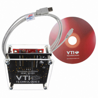
SCC1300-D04DEMO
Manufacturer Part Number
SCC1300-D04DEMO
Description
DEMO KIT WITH SCC1300-D04
Manufacturer
VTI Technologies
Datasheet
1.SCC1300-D04_PWB.pdf
(30 pages)
Specifications of SCC1300-D04DEMO
Sensor Type
Accelerometer, Gyroscope, 3 Axis
Sensing Range
±6g;, ±300°/sec
Interface
SPI
Sensitivity
Gyro: 18 LSB/(°/s), ±0.1 (°/s)/g Accel: 650LSB/g
Embedded
No
Utilized Ic / Part
SCC1300-D04
Lead Free Status / RoHS Status
Lead free / RoHS Compliant
Voltage - Supply
-
Other names
551-1070
SCC1300-D02DEMO
SCC1300-D02DEMO


4.4 Accelerometer Interface
4.4.1
VTI Technologies Oy
www.vti.fi
Output of Acceleration Data
This chapter describes the SCC1300 accelerometer part SPI interface and how to use it. SPI frame
format and transfer protocol for SCC1300 accelerometer ASIC is presented in Figure 8.
Figure 8. SPI frame format for accelerometer interface.
•
•
Each communication frame contains 16 bits. Each output data/status-bits are shifted out on the
falling edge of SCK (MISO line). Each bit is sampled on the rising edge of SCK (MOSI line).
address being accessed. First 6 bits define 6 bit address for selected operation, which is defined
by bit 7 (‘0’ = read ‘1’ = write), which is followed by odd parity bit (aPAR) for 8 bit pattern. The later
8 bits in MOSI_A line contain data for a write operation and are ignored in case of read operation.
The first bits in MISO_A line are frame error bit (FRME, bit2) of previous frame, reset status bit
(PORST, bit3), self-test status bit (ST, bit4), saturation status (SAT, bit5), fixed zero bit (bit6), fixed
one bit (bit7) and odd parity bit of output data (dPAR, bit8)). Parity is calculated from data, which is
currently sent. The later 8 bits contain data for a read operation. During the write operation, these
data bits are previous data bits of addressed register.
For write commands, data is written into the addressed register on the rising edge of CSB_A. If the
command frame is invalid, data will not be written into the register.
The output register is shifted out MSB first over MISO_A output. Attempt to read a reserved
register outputs data of 00h.
When CSB is high state between data transfers, MISO_A line is in high-impedance state. If bit
CTRL.SDODIS is set to ‘1’, MISO_A line is always in high-impedance state. In multi-chip SPI bus
master can send data to all slave chips simultaneously.
16-bit data is sent in 8-bit data bytes during two frames. Each frame contains odd parity bit of data
bits. Number format of acceleration data is two’s complement number.
The first 8 bits in MOSI_A line contains info about the operation (read/write) and the register
MOSI_A
MISO_A
•
•
•
•
•
•
•
•
•
•
•
A5:A0
RB/W
aPAR
DI7:DI0
Bit 1
FRME
Bit 3-5 status bits
Bit 6
Bit 7
dPAR
DO7:DO0
•
•
•
PORST Power On Reset Status
ST
SAT
Doc.Nr. 82 1131 00 A
Subject to changes
Register address
Read/Write selection, '0'=read
Odd parity for bits A5:A0, RB/W
Input data for data write
not defined bit
Frame error indication (previous frame)
Self Test error
Output SATuration indicator
always ‘0’, fixed bit
always ‘1’, fixed bit
Odd parity for output data (DO7:DO0)
Output data
SCC1300-D04
Rev. 1.0
16/30
Related parts for SCC1300-D04DEMO
Image
Part Number
Description
Manufacturer
Datasheet
Request
R

Part Number:
Description:
GYRO/ACC COMBO 3-AXIS +/-2G SPI
Manufacturer:
VTI Technologies
Datasheet:

Part Number:
Description:
GYRO/ACC COMBO 3-AXIS +/-6G SPI
Manufacturer:
VTI Technologies
Datasheet:

Part Number:
Description:
ACCELEROMETER SGL 1.7G DIL8 SMD
Manufacturer:
VTI Technologies
Datasheet:

Part Number:
Description:
VTI Automotive Digital Accelerometer Platform
Manufacturer:
VTI [VTI technologies]
Datasheet:

Part Number:
Description:
BOARD PWB ACCEL 3-AXIS SPI/I2C
Manufacturer:
VTI Technologies
Datasheet:

Part Number:
Description:
EVAL BOARD ACCELEROMETER Y-AXIS
Manufacturer:
VTI Technologies
Datasheet:

Part Number:
Description:
EVAL BOARD INCLINOMETER Y-AXIS
Manufacturer:
VTI Technologies
Datasheet:

Part Number:
Description:
KIT DEMO ACCELEROMTR CMA3000-D01
Manufacturer:
VTI Technologies
Datasheet:

Part Number:
Description:
KIT DEMO ACCELEROMTR SCA3060-D01
Manufacturer:
VTI Technologies
Datasheet:

Part Number:
Description:
BOARD PWB ACCEL 3AXIS ANALG OUT
Manufacturer:
VTI Technologies
Datasheet:
Part Number:
Description:
ACCELEROMETER SGL 1.7G DIL8 SMD
Manufacturer:
VTI Technologies
Datasheet:
Part Number:
Description:
VTI Automotive Digital Accelerometer Platform
Manufacturer:
VTI [VTI technologies]
Datasheet:
Part Number:
Description:
Accelerometer
Manufacturer:
VTI [VTI technologies]
Datasheet:
Part Number:
Description:
Stand Alone Inclinometer
Manufacturer:
VTI [VTI technologies]
Datasheet:
Part Number:
Description:
3-axis accelerometer
Manufacturer:
VTI [VTI technologies]
Datasheet: