DV164136 Microchip Technology, DV164136 Datasheet - Page 104
DV164136
Manufacturer Part Number
DV164136
Description
DEVELOPMENT KIT FOR PIC18
Manufacturer
Microchip Technology
Series
PIC®r
Type
MCUr
Datasheets
1.DM183032.pdf
(38 pages)
2.DV164136.pdf
(448 pages)
3.DV164136.pdf
(6 pages)
4.DV164136.pdf
(446 pages)
5.DV164136.pdf
(4 pages)
6.DV164136.pdf
(18 pages)
Specifications of DV164136
Contents
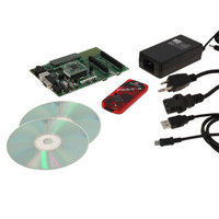
Board, Cables, CDs, PICkit™ 3 Programmer, Power Supply
Processor To Be Evaluated
PIC18F8722, PIC18F87J11
Interface Type
RS-232, USB
Operating Supply Voltage
3.3 V, 5 V
Silicon Manufacturer
Microchip
Core Architecture
PIC
Core Sub-architecture
PIC18
Silicon Core Number
PIC18F
Silicon Family Name
PIC18F8xxx
Kit Contents
PIC18 Exp Brd PICkit 3 Cable CD PSU
Lead Free Status / RoHS Status
Lead free / RoHS Compliant
For Use With/related Products
PIC18F8722, PIC18F87J11
Lead Free Status / Rohs Status
Lead free / RoHS Compliant
Available stocks
Company
Part Number
Manufacturer
Quantity
Price
Company:

Part Number:
DV164136
Manufacturer:
MICROCHIP
Quantity:
12 000


PIC18F8722 FAMILY
7.5.2
Figure 7-2 shows an example of 16-bit Word Write
mode for PIC18F8527/8622/8627/8722 devices. This
mode is used for word-wide memories which includes
some of the EPROM and Flash-type memories. This
mode allows opcode fetches and table reads from all
forms of 16-bit memory and table writes to any type of
word-wide external memories. This method makes a
distinction between TBLWT cycles to even or odd
addresses.
During
(TBLPTR<0> = 0), the TABLAT data is transferred to a
holding latch and the external address data bus is
tri-stated for the data portion of the bus cycle. No write
signals are activated.
FIGURE 7-2:
DS39646C-page 102
Note 1:
a
PIC18F8X27/8X22
16-BIT WORD WRITE MODE
TBLWT
2:
A<19:16>
AD<15:8>
Upper-order address lines are used only for 20-bit address widths.
This signal only applies to table writes. See Section 6.1 “Table Reads and Table Writes”.
AD<7:0>
cycle
16-BIT WORD WRITE MODE EXAMPLE
WRH
ALE
OE
CE
(1)
to
an
even
address
373
373
During
(TBLPTR<0> = 1), the TABLAT data is presented on
the upper byte of the AD15:AD0 bus. The contents of
the holding latch are presented on the lower byte of the
AD<15:0> bus.
The WRH signal is strobed for each write cycle; the
WRL pin is unused. The signal on the BA0 pin indicates
the Least Significant bit of TBLPTR but it is left
unconnected. Instead, the UB and LB signals are
active to select both bytes. The obvious limitation to
this method is that the table write must be done in pairs
on a specific word boundary to correctly write a word
location.
A<20:1>
D<15:0>
a
TBLWT
Address Bus
Data Bus
Control Lines
D<15:0>
A<x:0>
cycle
CE
© 2008 Microchip Technology Inc.
EPROM Memory
to
OE
JEDEC Word
an
WR
odd
(2)
address
Related parts for DV164136
Image
Part Number
Description
Manufacturer
Datasheet
Request
R

Part Number:
Description:
Manufacturer:
Microchip Technology Inc.
Datasheet:
Part Number:
Description:
Manufacturer:
Microchip Technology Inc.
Datasheet:
Part Number:
Description:
Manufacturer:
Microchip Technology Inc.
Datasheet:
Part Number:
Description:
Manufacturer:
Microchip Technology Inc.
Datasheet:
Part Number:
Description:
Manufacturer:
Microchip Technology Inc.
Datasheet:
Part Number:
Description:
Manufacturer:
Microchip Technology Inc.
Datasheet:
Part Number:
Description:
Manufacturer:
Microchip Technology Inc.
Datasheet:
Part Number:
Description:
Manufacturer:
Microchip Technology Inc.
Datasheet: