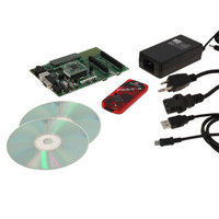
DV164136 Microchip Technology, DV164136 Datasheet - Page 105

DV164136
Manufacturer Part Number
DV164136
Description
DEVELOPMENT KIT FOR PIC18
Manufacturer
Microchip Technology
Series
PIC®r
Type
MCUr
Datasheets
1.DM183032.pdf
(38 pages)
2.DV164136.pdf
(448 pages)
3.DV164136.pdf
(6 pages)
4.DV164136.pdf
(446 pages)
5.DV164136.pdf
(4 pages)
6.DV164136.pdf
(18 pages)
Specifications of DV164136
Contents
Board, Cables, CDs, PICkit™ 3 Programmer, Power Supply
Processor To Be Evaluated
PIC18F8722, PIC18F87J11
Interface Type
RS-232, USB
Operating Supply Voltage
3.3 V, 5 V
Silicon Manufacturer
Microchip
Core Architecture
PIC
Core Sub-architecture
PIC18
Silicon Core Number
PIC18F
Silicon Family Name
PIC18F8xxx
Kit Contents
PIC18 Exp Brd PICkit 3 Cable CD PSU
Lead Free Status / RoHS Status
Lead free / RoHS Compliant
For Use With/related Products
PIC18F8722, PIC18F87J11
Lead Free Status / Rohs Status
Lead free / RoHS Compliant
Available stocks
Company
Part Number
Manufacturer
Quantity
Price
Company:
Part Number:
DV164136
Manufacturer:
MICROCHIP
Quantity:
12 000
- DM183032 PDF datasheet
- DV164136 PDF datasheet #2
- DV164136 PDF datasheet #3
- DV164136 PDF datasheet #4
- DV164136 PDF datasheet #5
- DV164136 PDF datasheet #6
- Current page: 105 of 446
- Download datasheet (7Mb)
7.5.3
Figure 7-3 shows an example of 16-bit Byte Select
mode. This mode allows table write operations to
word-wide external memories with byte selection
capability. This generally includes both word-wide
Flash and SRAM devices.
During a TBLWT cycle, the TABLAT data is presented
on the upper and lower byte of the AD<15:0> bus. The
WRH signal is strobed for each write cycle; the WRL
pin is not used. The BA0 or UB/LB signals are used to
select the byte to be written, based on the Least
Significant bit of the TBLPTR register.
FIGURE 7-3:
© 2008 Microchip Technology Inc.
Note 1:
PIC18F8X27/8X22
2:
3:
16-BIT BYTE SELECT MODE
A<19:16>
AD<15:8>
AD<7:0>
This signal only applies to table writes. See Section 6.1 “Table Reads and Table Writes”.
Upper-order address lines are used only for 20-bit address width.
Demultiplexing is only required when multiple memory devices are accessed.
WRH
WRL
ALE
BA0
OE
UB
I/O
LB
(2)
16-BIT BYTE SELECT MODE EXAMPLE
373
373
A<20:1>
A<20:1>
138
Flash and SRAM devices use different control signal
combinations to implement Byte Select mode. JEDEC
standard Flash memories require that a controller I/O
port pin be connected to the memory’s BYTE/WORD
pin to provide the select signal. They also use the BA0
signal from the controller as a byte address. JEDEC
standard static RAM memories, on the other hand, use
the UB or LB signals to select the byte.
PIC18F8722 FAMILY
(3)
A<x:1>
A<x:1>
CE
A0
CE
UB
BYTE/WORD
LB
OE
SRAM Memory
Flash Memory
WR
JEDEC Word
JEDEC Word
Address Bus
Data Bus
Control Lines
OE WR
(1)
D<15:0>
D<15:0>
DS39646C-page 103
(1)
D<15:0>
D<15:0>
Related parts for DV164136
Image
Part Number
Description
Manufacturer
Datasheet
Request
R

Part Number:
Description:
Manufacturer:
Microchip Technology Inc.
Datasheet:

Part Number:
Description:
Manufacturer:
Microchip Technology Inc.
Datasheet:

Part Number:
Description:
Manufacturer:
Microchip Technology Inc.
Datasheet:

Part Number:
Description:
Manufacturer:
Microchip Technology Inc.
Datasheet:

Part Number:
Description:
Manufacturer:
Microchip Technology Inc.
Datasheet:

Part Number:
Description:
Manufacturer:
Microchip Technology Inc.
Datasheet:

Part Number:
Description:
Manufacturer:
Microchip Technology Inc.
Datasheet:

Part Number:
Description:
Manufacturer:
Microchip Technology Inc.
Datasheet:


