DV164136 Microchip Technology, DV164136 Datasheet - Page 221
DV164136
Manufacturer Part Number
DV164136
Description
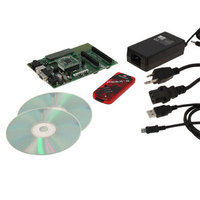
DEVELOPMENT KIT FOR PIC18
Manufacturer
Microchip Technology
Series
PIC®r
Type
MCUr
Datasheets
1.DM183032.pdf
(38 pages)
2.DV164136.pdf
(448 pages)
3.DV164136.pdf
(6 pages)
4.DV164136.pdf
(446 pages)
5.DV164136.pdf
(4 pages)
6.DV164136.pdf
(18 pages)
Specifications of DV164136
Contents
Board, Cables, CDs, PICkit™ 3 Programmer, Power Supply
Processor To Be Evaluated
PIC18F8722, PIC18F87J11
Interface Type
RS-232, USB
Operating Supply Voltage
3.3 V, 5 V
Silicon Manufacturer
Microchip
Core Architecture
PIC
Core Sub-architecture
PIC18
Silicon Core Number
PIC18F
Silicon Family Name
PIC18F8xxx
Kit Contents
PIC18 Exp Brd PICkit 3 Cable CD PSU
Lead Free Status / RoHS Status
Lead free / RoHS Compliant
For Use With/related Products
PIC18F8722, PIC18F87J11
Lead Free Status / Rohs Status
Lead free / RoHS Compliant
Available stocks
Company
Part Number
Manufacturer
Quantity
Price
Company:

Part Number:
DV164136
Manufacturer:
MICROCHIP
Quantity:
12 000


19.4.2
The MSSP module functions are enabled by setting
MSSP Enable bit, SSPEN (SSPxCON1<5>).
The SSPxCON1 register allows control of the I
operation. Four mode selection bits (SSPxCON1<3:0>)
allow one of the following I
• I
• I
• I
• I
• I
• I
Selection of any I
forces the SCLx and SDAx pins to be open-drain,
provided these pins are programmed as inputs by
setting the appropriate TRISC or TRISD bits. To ensure
proper operation of the module, pull-up resistors must
be provided externally to the SCLx and SDAx pins.
19.4.3
In Slave mode, the SCLx and SDAx pins must be
configured as inputs (TRISC<4:3> set). The MSSP
module will override the input state with the output data
when required (slave-transmitter).
The I
interrupt on an address match. Through the mode
select bits, the user can also choose to interrupt on
Start and Stop bits
When an address is matched, or the data transfer after
an address match is received, the hardware auto-
matically will generate the Acknowledge (ACK) pulse
and load the SSPxBUF register with the received value
currently in the SSPxSR register.
Any combination of the following conditions will cause
the MSSP module not to give this ACK pulse:
• The Buffer Full bit, BF (SSPxSTAT<0>), was set
• The overflow bit, SSPOV (SSPxCON1<6>), was
In this case, the SSPxSR register value is not loaded
into the SSPxBUF, but bit SSPxIF is set. The BF bit is
cleared by reading the SSPxBUF register, while bit
SSPOV is cleared through software.
The SCLx clock input must have a minimum high and
low for proper operation. The high and low times of the
I
MSSP module, are shown in timing parameter 100 and
parameter 101.
© 2008 Microchip Technology Inc.
2
C specification, as well as the requirement of the
Stop bit interrupts enabled
Stop bit interrupts enabled
Idle
before the transfer was received.
set before the transfer was received.
2
2
2
2
2
2
C Master mode, clock
C Slave mode (7-bit address)
C Slave mode (10-bit address)
C Slave mode (7-bit address) with Start and
C Slave mode (10-bit address) with Start and
C Firmware Controlled Master mode, slave is
2
C Slave mode hardware will always generate an
OPERATION
SLAVE MODE
2
C mode with the SSPEN bit set
2
C modes to be selected:
2
C
19.4.3.1
Once the MSSP module has been enabled, it waits for
a Start condition to occur. Following the Start condition,
the 8 bits are shifted into the SSPxSR register. All
incoming bits are sampled with the rising edge of the
clock (SCLx) line. The value of register SSPxSR<7:1>
is compared to the value of the SSPxADD register. The
address is compared on the falling edge of the eighth
clock (SCLx) pulse. If the addresses match and the BF
and SSPOV bits are clear, the following events occur:
1.
2.
3.
4.
In 10-Bit Addressing mode, two address bytes need to
be received by the slave. The five Most Significant bits
(MSbs) of the first address byte specify if this is a 10-bit
address. Bit R/W (SSPxSTAT<2>) must specify a write
so the slave device will receive the second address byte.
For a 10-bit address, the first byte would equal ‘11110
A9 A8 0’, where ‘A9’ and ‘A8’ are the two MSbs of the
address. The sequence of events for 10-bit address is as
follows, with steps 7 through 9 for the slave-transmitter:
1.
2.
3.
4.
5.
6.
7.
8.
9.
PIC18F8722 FAMILY
The SSPxSR register value is loaded into the
SSPxBUF register.
The Buffer Full bit, BF, is set.
An ACK pulse is generated.
The MSSP Interrupt Flag bit, SSPxIF, is set (and
interrupt is generated, if enabled) on the falling
edge of the ninth SCLx pulse.
Receive first (high) byte of address (bits SSPxIF,
BF and UA (SSPxSTAT<1>) are set on address
match).
Update the SSPxADD register with second (low)
byte of address (clears bit UA and releases the
SCLx line).
Read the SSPxBUF register (clears bit BF) and
clear flag bit SSPxIF.
Receive second (low) byte of address (bits
SSPxIF, BF and UA are set).
Update the SSPxADD register with the first
(high) byte of address. If match releases SCLx
line, this will clear bit UA.
Read the SSPxBUF register (clears bit BF) and
clear flag bit SSPxIF.
Receive Repeated Start condition.
Receive first (high) byte of address (bits SSPxIF
and BF are set).
Read the SSPxBUF register (clears bit BF) and
clear flag bit SSPxIF.
Addressing
DS39646C-page 219
Related parts for DV164136
Image
Part Number
Description
Manufacturer
Datasheet
Request
R

Part Number:
Description:
Manufacturer:
Microchip Technology Inc.
Datasheet:
Part Number:
Description:
Manufacturer:
Microchip Technology Inc.
Datasheet:
Part Number:
Description:
Manufacturer:
Microchip Technology Inc.
Datasheet:
Part Number:
Description:
Manufacturer:
Microchip Technology Inc.
Datasheet:
Part Number:
Description:
Manufacturer:
Microchip Technology Inc.
Datasheet:
Part Number:
Description:
Manufacturer:
Microchip Technology Inc.
Datasheet:
Part Number:
Description:
Manufacturer:
Microchip Technology Inc.
Datasheet:
Part Number:
Description:
Manufacturer:
Microchip Technology Inc.
Datasheet: