DV164136 Microchip Technology, DV164136 Datasheet - Page 222
DV164136
Manufacturer Part Number
DV164136
Description
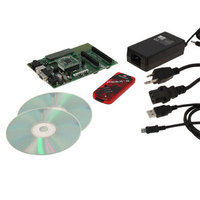
DEVELOPMENT KIT FOR PIC18
Manufacturer
Microchip Technology
Series
PIC®r
Type
MCUr
Datasheets
1.DM183032.pdf
(38 pages)
2.DV164136.pdf
(448 pages)
3.DV164136.pdf
(6 pages)
4.DV164136.pdf
(446 pages)
5.DV164136.pdf
(4 pages)
6.DV164136.pdf
(18 pages)
Specifications of DV164136
Contents
Board, Cables, CDs, PICkit™ 3 Programmer, Power Supply
Processor To Be Evaluated
PIC18F8722, PIC18F87J11
Interface Type
RS-232, USB
Operating Supply Voltage
3.3 V, 5 V
Silicon Manufacturer
Microchip
Core Architecture
PIC
Core Sub-architecture
PIC18
Silicon Core Number
PIC18F
Silicon Family Name
PIC18F8xxx
Kit Contents
PIC18 Exp Brd PICkit 3 Cable CD PSU
Lead Free Status / RoHS Status
Lead free / RoHS Compliant
For Use With/related Products
PIC18F8722, PIC18F87J11
Lead Free Status / Rohs Status
Lead free / RoHS Compliant
Available stocks
Company
Part Number
Manufacturer
Quantity
Price
Company:

Part Number:
DV164136
Manufacturer:
MICROCHIP
Quantity:
12 000


PIC18F8722 FAMILY
19.4.3.2
When the R/W bit of the address byte is clear and an
address match occurs, the R/W bit of the SSPxSTAT
register is cleared. The received address is loaded into
the SSPxBUF register and the SDAx line is held low
(ACK).
When the address byte overflow condition exists, then
the no Acknowledge (ACK) pulse is given. An overflow
condition is defined as either bit BF (SSPxSTAT<0>) is
set, or bit SSPOV (SSPxCON1<6>) is set.
An MSSP interrupt is generated for each data transfer
byte. The interrupt flag bit, SSPxIF, must be cleared in
software. The SSPxSTAT register is used to determine
the status of the byte.
If SEN is enabled (SSPxCON2<0> = 1), SCLx will be
held low (clock stretch) following each data transfer. The
clock
(SSPxCON1<4>).
Stretching” for more detail.
DS39646C-page 220
must
Reception
be
released
See
Section 19.4.4
by
setting
bit,
“Clock
CKP
19.4.3.3
When the R/W bit of the incoming address byte is set
and an address match occurs, the R/W bit of the
SSPxSTAT register is set. The received address is
loaded into the SSPxBUF register. The ACK pulse will
be sent on the ninth bit and pin SCLx is held low regard-
less of SEN (see Section 19.4.4 “Clock Stretching”
for more detail). By stretching the clock, the master will
be unable to assert another clock pulse until the slave
is done preparing the transmit data. The transmit data
must be loaded into the SSPxBUF register which also
loads the SSPxSR register. Then pin SCLx should be
enabled by setting bit, CKP (SSPxCON1<4>). The
eight data bits are shifted out on the falling edge of the
SCLx input. This ensures that the SDAx signal is valid
during the SCLx high time (Figure 19-9).
The ACK pulse from the master-receiver is latched on
the rising edge of the ninth SCLx input pulse. If the
SDAx line is high (not ACK), then the data transfer is
complete. In this case, when the ACK is latched by the
slave, the slave logic is reset (resets SSPxSTAT
register) and the slave monitors for another occurrence
of the Start bit. If the SDAx line was low (ACK), the next
transmit data must be loaded into the SSPxBUF
register. Again, pin SCLx must be enabled by setting bit
CKP.
An MSSP interrupt is generated for each data transfer
byte. The SSPxIF bit must be cleared in software and
the SSPxSTAT register is used to determine the status
of the byte. The SSPxIF bit is set on the falling edge of
the ninth clock pulse.
Transmission
© 2008 Microchip Technology Inc.
Related parts for DV164136
Image
Part Number
Description
Manufacturer
Datasheet
Request
R

Part Number:
Description:
Manufacturer:
Microchip Technology Inc.
Datasheet:
Part Number:
Description:
Manufacturer:
Microchip Technology Inc.
Datasheet:
Part Number:
Description:
Manufacturer:
Microchip Technology Inc.
Datasheet:
Part Number:
Description:
Manufacturer:
Microchip Technology Inc.
Datasheet:
Part Number:
Description:
Manufacturer:
Microchip Technology Inc.
Datasheet:
Part Number:
Description:
Manufacturer:
Microchip Technology Inc.
Datasheet:
Part Number:
Description:
Manufacturer:
Microchip Technology Inc.
Datasheet:
Part Number:
Description:
Manufacturer:
Microchip Technology Inc.
Datasheet: