EVAL-ADUC7128QSPZ Analog Devices Inc, EVAL-ADUC7128QSPZ Datasheet - Page 6
EVAL-ADUC7128QSPZ
Manufacturer Part Number
EVAL-ADUC7128QSPZ
Description
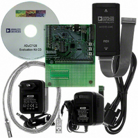
KIT DEV FOR ADUC7128
Manufacturer
Analog Devices Inc
Series
QuickStart™ PLUS Kitr
Type
MCUr
Datasheet
1.EVAL-ADUC7128QSPZ.pdf
(92 pages)
Specifications of EVAL-ADUC7128QSPZ
Contents
Evaluation Board, Power Supply, Cable, Software, Emulator and Documentation
Silicon Manufacturer
Analog Devices
Core Architecture
ARM
Core Sub-architecture
ARM7TDMI
Silicon Core Number
ADuC7128
Rohs Compliant
Yes
Lead Free Status / RoHS Status
Lead free / RoHS Compliant
For Use With/related Products
ADuC7128
Lead Free Status / RoHS Status
Lead free / RoHS Compliant, Lead free / RoHS Compliant


ADuC7128/ADuC7129
Parameter
LOGIC INPUTS
LOGIC OUTPUTS
CRYSTAL INPUTS XCLKI and XCLKO
MCU CLOCK RATE (PLL)
INTERNAL OSCILLATOR
STARTUP TIME
PROGRAMMABLE LOGIC ARRAY (PLA)
POWER REQUIREMENTS
1
2
3
4
5
6
7
8
9
10
supply, sleep mode = 3.6 V supply.
11
All ADC channel specifications are guaranteed during normal MicroConverter core operation.
Apply to all ADC input channels.
Not production tested; supported by design and/or characterization of data on production release.
Measured using an external
The input signal can be centered on any dc common-mode voltage (V
When using an external reference input pin, the internal reference must be disabled by setting the LSB in the REFCON memory mapped register to 0.
Endurance is qualified as per JEDEC Std. 22 Method A117 and measured at −40°C, +25°C, and +85°C.
Retention lifetime equivalent at junction temperature (T
Test carried out with a maximum of eight I/Os set to a low output level.
Power supply current consumption is measured in normal, pause, and sleep modes under the following conditions: normal mode = 3.6 V supply, pause mode = 3.6 V
IOV
V
V
V
V
At Power-On
From Sleep Mode
From Stop Mode
Pin Propagation Delay
Element Propagation Delay
Power Supply Voltage Range
Quadrature Encoder Inputs
S1/S2/CLR (Schmitt-Triggered Inputs)
V
V
XCLKI, Input Capacitance
XCLKO, Output Capacitance
Tolerance
Power Supply Current
INL
INH
INL
INH
OH
OL
DD
IOV
Normal Mode
Additional Line Driver Tx Supply
V
V
V
LV
Pause Mode
Sleep Mode
, Output Low Voltage
, Input Low Voltage
, Output High Voltage
, Input Low Voltage
, Input High Voltage
, Input High Voltage
T+
T−
T+
power supply current decreases typically by 2 mA during a Flash/EE erase cycle.
DD
Voltage to Chip)
Current
DD
− V
(Regulator Output from Chip)
, AV
T−
3
DD
, and DACV
9
10, 11
AD845
DD
(Supply
op amp as an input buffer stage, as shown in Figure 42. Based on external ADC system components.
Min
2.0
IOV
400 mV
326.4
3.0
2.5
DD
−
J
) = 85°C as per JEDEC Std. 22 Method A117. Retention lifetime derates with junction temperature.
Typ
1.65
1.2
0.75
1.1
1.7
20
20
32.768
70
1.6
1.6
12
2.5
2.6
15
42
0.3
CM
), as long as this value is within the ADC voltage input range specified.
Rev. 0 | Page 6 of 92
Max
0.8
0.4
41.77920
±3
±4
3.6
2.7
19
49
30
37
3.6
Unit
V
V
V
V
V
V
V
V
V
pF
pF
kHz
MHz
kHz
%
ms
ms
ms
ns
ns
V
V
mA
mA
mA
mA
mA
%
Test Conditions/Comments
All logic inputs, including XCLKI and XCLKO
I
I
Logic inputs, XCLKI only
Logic inputs, XCLKI only
Eight programmable core clock selections
within this range
(32.768 kHz x 1275)/128
(32.768 kHz x 1275)/1
−40°C to 85°C
85°C to 125°C only
Core clock = 41.78 MHz
From input pin to output pin
5.22 MHz clock
41.78 MHz clock
691 kHz, maximum load (see Figure 2)
41.78 MHz clock
External crystal or internal OSC ON
SOURCE
SINK
= 1.6 mA
= 1.6 mA
Related parts for EVAL-ADUC7128QSPZ
Image
Part Number
Description
Manufacturer
Datasheet
Request
R

Part Number:
Description:
IC, ADJ LDO REG, 1.5V TO 5V 250mA MSOP-8
Manufacturer:
Vishay
Datasheet:

Part Number:
Description:
IC, ADJ LDO REG, 1.5V TO 5V 0.6A 8-TSSOP
Manufacturer:
Vishay
Datasheet:
Part Number:
Description:
IC, ADJ LDO REG, 1.5V TO 5V 250mA MSOP-8
Manufacturer:
Vishay
Datasheet:

Part Number:
Description:
IC ADJ LDO REG 1.5V TO 5V 150mA 5-SOT-23
Manufacturer:
Vishay
Datasheet:

Part Number:
Description:
BOARD EVAL AS1324-AD
Manufacturer:
austriamicrosystems
Datasheet:
Part Number:
Description:
IC, ADJ LDO REG, 1.5V TO 5V 0.6A 8-TSSOP
Manufacturer:
Vishay
Datasheet:

Part Number:
Description:
IC, ADJ LDO REG, 1.5V TO 5V, 0.3A, MSOP8
Manufacturer:
Vishay
Datasheet:
Part Number:
Description:
IC, ADJ LDO REG, 1.5V TO 5V, 0.3A, MSOP8
Manufacturer:
Vishay
Datasheet:
Part Number:
Description:
IC, ADJ LDO REG 1.215V TO 5V 0.3A MSOP-8
Manufacturer:
Vishay
Datasheet:
Part Number:
Description:
IC, ADJ LDO REG 1.215V TO 5V 0.3A MSOP-8
Manufacturer:
Vishay
Datasheet:

Part Number:
Description:
±1.7g Dual-Axis IMEMS Accelerometer Evaluation Board
Manufacturer:
Analog Devices Inc
Datasheet:

Part Number:
Description:
IC MULTIPLIER ANALOG 8-SOIC T/R
Manufacturer:
Analog Devices Inc
Datasheet:

Part Number:
Description:
IC ANALOG MULTIPLIER 8-DIP
Manufacturer:
Analog Devices Inc
Datasheet:
Part Number:
Description:
IC ANALOG MULTIPLIER 8-SOIC
Manufacturer:
Analog Devices Inc
Datasheet:
Part Number:
Description:
IC ANALOG MULTIPLIER 8-DIP
Manufacturer:
Analog Devices Inc
Datasheet: