XE8000EV110 Semtech, XE8000EV110 Datasheet - Page 170
XE8000EV110
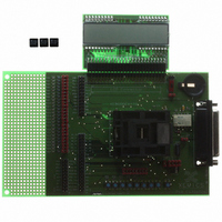
Manufacturer Part Number
XE8000EV110
Description
EVAL BOARD FOR XE8802AMI035LF
Manufacturer
Semtech
Type
MCUr
Specifications of XE8000EV110
Contents
Fully Assembled Evaluation Board
For Use With/related Products
XE88LC02MI035
Lead Free Status / RoHS Status
Contains lead / RoHS non-compliant


19.7.2
When configured as a digital I/O, the logical ‘1’ on the pins pad_lcd_io[31:0] is identical to V3. For a part of the
pad_lcd_io[31:0] pins, the V3 connection is not made inside the circuit but has to be done externally by connecting
the pins pad_vgen_v3, pad_lcd_vr1 and pad_lcd_vr2 together. This feature allows for the use of different voltages
on V3 for the LCD display and for I/O parallel pins. Table 19-28 shows the partitioning of the pins. The voltages that
can be applied on pad_vgen_v3, pad_lcd_vr1, pad_lcd_vr2 and VBAT are completely independent from each
other.
© Semtech 2006
Different Voltages for V3 of LCD and Digital I/O
Figure 19-21. Sharing LCD driver (1:4 mux) and digital I/O with V3 ≠ logic ‘1’
VGEN
1.2V voltage
reference
Table 19-28. V3 connection of the different pad_lcd_io pins
pad_lcd_com0
pad_lcd_com1
pad_lcd_io[31:12]
pad_lcd_io[11:4]
pad_lcd_io[3:0]
pad_lcd_io[29:12]
pad_lcd_io[30]
pad_lcd_io[31]
pad_lcd_com1
pad_lcd_com0
pad_lcd_io[11:4]
pad_vgen_vb
pad_vgen_v3
pad_vgen_v2
pad_vgen_v1
pad_vgen_va
pad_lcd_io[3:0]
pad_lcd_vr2
pad_lcd_vr1
vdd1 voltage domain
vdd2 voltage domain
vbat
vss
XE8802 Sensing Machine Data Acquisition MCU
pin
SEGMENTS[17:0]
C
lcd1
COM3
COM2
COM1
COM0
19-26
C
vbat
vdd1
vdd2
lcd2
V3 connection
pad_vgen_v3
pad_lcd_vr1
pad_lcd_vr2
C
with ZoomingADC™ and LCD driver
lcd3
vdd
io[3:0]
vdd
io[7:0]
C
aux
LCD DISPLAY
EXTERNAL
CIRCUIT
EXTERNAL
CIRCUIT
vss
vss
www.semtech.com
Related parts for XE8000EV110
Image
Part Number
Description
Manufacturer
Datasheet
Request
R

Part Number:
Description:
EVALUATION BOARD
Manufacturer:
Semtech
Datasheet:
Part Number:
Description:
EVALUATION BOARD
Manufacturer:
Semtech
Datasheet:
Part Number:
Description:
VOLTAGE SUPPRESSOR, TRANSIENT SEMTECH
Manufacturer:
Semtech
Datasheet:

Part Number:
Description:
HIGH VOLTAGE CAPACITORS MONOLITHIC CERAMIC TYPE
Manufacturer:
Semtech Corporation
Datasheet:
Part Number:
Description:
EZ1084CM5.0 AMP POSITIVE VOLTAGE REGULATOR
Manufacturer:
Semtech Corporation
Datasheet:
Part Number:
Description:
3.0 AMP LOW DROPOUT POSITIVE VOLTAGE REGULATORS
Manufacturer:
Semtech Corporation
Datasheet:
Part Number:
Description:
Manufacturer:
Semtech Corporation
Datasheet:
Part Number:
Description:
RailClamp Low Capacitance TVS Diode Array
Manufacturer:
Semtech Corporation
Datasheet:
Part Number:
Description:
Manufacturer:
Semtech Corporation
Datasheet:
Part Number:
Description:
Manufacturer:
Semtech Corporation
Datasheet:
Part Number:
Description:
Manufacturer:
Semtech Corporation
Datasheet:
Part Number:
Description:
Manufacturer:
Semtech Corporation
Datasheet: