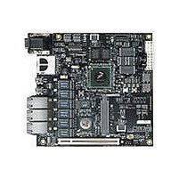
MPC8313E-RDBB Freescale Semiconductor, MPC8313E-RDBB Datasheet - Page 36

MPC8313E-RDBB
Manufacturer Part Number
MPC8313E-RDBB
Description
BOARD CPU 8313E VER 2.1
Manufacturer
Freescale Semiconductor
Series
PowerQUICC II™ PROr
Type
MPUr
Datasheets
1.MPC8313CZQAFFB.pdf
(100 pages)
2.MPC8313E-RDBB.pdf
(52 pages)
3.MPC8313E-RDBB.pdf
(2 pages)
Specifications of MPC8313E-RDBB
Contents
Board
Processor To Be Evaluated
MPC8xxx
Data Bus Width
32 bit
Interface Type
Ethernet, USB, JTAG, SPI, UART
Dimensions
170 mm x 170 mm
Operating Supply Voltage
3.3 V
For Use With/related Products
MPC8313E
Lead Free Status / RoHS Status
Lead free / RoHS Compliant
High-Speed Serial Interfaces (HSSI)
Figure 21
9
This section describes the common portion of SerDes DC electrical specifications, which is the DC
requirement for SerDes reference clocks. The SerDes data lane’s transmitter and receiver reference circuits
are also shown.
9.1
The SerDes utilizes differential signaling to transfer data across the serial link. This section defines terms
used in the description and specification of differential signals.
Figure 22
description. The figure shows waveform for either a transmitter output (TXn and TXn) or a receiver input
(RXn and RXn). Each signal swings between A volts and B volts where A > B.
Using this waveform, the definitions are as follows. To simplify illustration, the following definitions
assume that the SerDes transmitter and receiver operate in a fully symmetrical differential signaling
environment.
36
1. Single-ended swing
2. Differential output voltage, V
3. Differential input voltage, V
High-Speed Serial Interfaces (HSSI)
The transmitter output signals and the receiver input signals TXn, TXn, RXn, and RXn each have
a peak-to-peak swing of A – B volts. This is also referred as each signal wire’s single-ended swing.
The differential output voltage (or swing) of the transmitter, V
the two complimentary output voltages: V
negative.
The differential input voltage (or swing) of the receiver, V
complimentary input voltages: V
Signal Terms Definition
shows the MII management AC timing diagram.
shows how the signals are defined. For illustration purpose, only one SerDes lane is used for
(Output)
(Input)
MDIO
MDIO
MPC8313E PowerQUICC
MDC
Figure 21. MII Management Interface Timing Diagram
t
MDCH
ID
t
MDDVKH
OD
t
(or differential input swing):
MDC
RXn
(or differential output swing):
™
t
MDKHDX
II Pro Processor Hardware Specifications, Rev. 3
– V
RXn
TXn
. The V
t
– V
MDCF
TXn.
ID
t
MDDXKH
The V
value can be either positive or negative.
t
ID
MDCR
, is defined as the difference of the two
OD
OD
value can be either positive or
, is defined as the difference of
Freescale Semiconductor


