DK-DEV-2AGX125N Altera, DK-DEV-2AGX125N Datasheet - Page 15
DK-DEV-2AGX125N
Manufacturer Part Number
DK-DEV-2AGX125N
Description
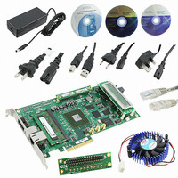
KIT DEV ARRIA II GX FPGA 2AGX125
Manufacturer
Altera
Series
Arria II GXr
Type
FPGAr
Datasheets
1.EP2AGX45CU17C6N.pdf
(96 pages)
2.DK-DEV-2AGX125N.pdf
(48 pages)
3.DK-DEV-2AGX125N.pdf
(64 pages)
Specifications of DK-DEV-2AGX125N
Contents
Board, Cables, CD, DVD, Power Supply
Silicon Manufacturer
Altera
Core Architecture
FPGA
Core Sub-architecture
Arria
Silicon Core Number
EP2
Silicon Family Name
Arria II GX
Rohs Compliant
Yes
For Use With/related Products
EP2AGX125EF35
Lead Free Status / RoHS Status
Lead free / RoHS Compliant
Other names
544-2600
Available stocks
Company
Part Number
Manufacturer
Quantity
Price
Company:

Part Number:
DK-DEV-2AGX125N
Manufacturer:
Altera
Quantity:
135


Chapter 1: Device Datasheet for Arria II Devices
Electrical Characteristics
Table 1–6. Recommended Operating Conditions for Arria II GZ Devices (Part 2 of 2)
December 2010 Altera Corporation
V
V
V
V
T
t
Notes to
(1) Altera recommends a 3.0-V nominal battery voltage when connecting V
(2) V
(3) n = 0, 1, or 2.
(4) V
(5) V
(6) Transceiver power supplies do not have power-on-reset (POR) circuitry. After initial power-up, violating the transceiver power supply operating
(3)
(3)
(3)
(3)
RAMP
J
CCL_GXBLn
CCL_GXBRn
CCH_GXBLn
CCH_GXBRn
Symbol
security key, you may connect the V
both, are configured at a base data rate > 4.25 Gbps. For data rates up to 4.25 Gbps, you can connect V
conditions could lead to unpredictable link behavior.
CCPD
CCA_L/R
CCH_GXBL/R
Table
must be 2.5 V when V
must be connected to a 3.0-V supply if the clock multiplier unit (CMU) phase-locked loop (PLL), receiver clock data recovery (CDR), or
Transceiver clock power (left side)
Transceiver clock power (right side)
Transmitter output buffer power (left side)
Transmitter output buffer power (right side)
Operating junction temperature
Power supply ramp time
1–6:
must be connected to a 1.5-V supply.
f
DC Characteristics
This section lists the supply current, I/O pin leakage current, on-chip termination
(OCT) accuracy and variation, input pin capacitance, internal weak pull-up and
pull-down resistance, hot socketing, and Schmitt trigger input specifications.
Supply Current
Standby current is the current the device draws after the device is configured with no
inputs or outputs toggling and no activity in the device. Because these currents vary
largely with the resources used, use the Microsoft Excel-based Early Power Estimator
(EPE) to get supply current estimates for your design.
For more information about power estimation tools, refer to the
Estimator User Guide
I/O Pin Leakage Current
Table 1–7
Table 1–7. I/O Pin Leakage Current for Arria II GX Devices
I
I
I
OZ
Symbol
CCIO
Description
is 2.5, 1.8, 1.5, or 1.2 V. V
CCBAT
lists the Arria II GX I/O pin leakage current specifications.
Input pin
Tri-stated I/O pin
to either GND or a 3.0-V power supply.
Description
and the
CCPD
PowerPlay Power Analysis
must be 3.0 V when V
V
V
I
O
Normal POR
(PORSEL=0)
(PORSEL=1)
= 0 V to V
Commercial
= 0 V to V
Condition
Industrial
Fast POR
CCBAT
Conditions
Arria II Device Handbook Volume 3: Device Datasheet and Addendum
—
—
—
—
to a battery for volatile key backup. If you do not use the volatile
CCIOMAX
CCIOMAX
CCIO
Minimum
is 3.0 V.
1.425
1.05
1.05
0.05
0.05
–40
0
chapter.
Min
–10
–10
(Note 6)
CCA_L/R
Typical
1.5
1.1
1.1
—
—
—
—
to either 3.0 V or 2.5 V.
(5)
PowerPlay Early Power
Typ
—
—
Maximum
1.575
Max
1.15
1.15
100
100
10
10
85
4
Unit
µA
µA
Unit
ms
ms
°C
°C
1–7
V
V
V
Related parts for DK-DEV-2AGX125N
Image
Part Number
Description
Manufacturer
Datasheet
Request
R

Part Number:
Description:
KIT DEV CYCLONE III LS EP3CLS200
Manufacturer:
Altera
Datasheet:

Part Number:
Description:
KIT DEV STRATIX IV FPGA 4SE530
Manufacturer:
Altera
Datasheet:

Part Number:
Description:
KIT DEV FPGA 2AGX260 W/6.375G TX
Manufacturer:
Altera
Datasheet:

Part Number:
Description:
KIT DEV MAX V 5M570Z
Manufacturer:
Altera
Datasheet:

Part Number:
Description:
KIT DEV STRATIX V FPGA 5SGXEA7
Manufacturer:
Altera
Datasheet:

Part Number:
Description:
KIT DEVELOPMENT STRATIX III
Manufacturer:
Altera
Datasheet:

Part Number:
Description:
KIT DEVELOPMENT STRATIX IV
Manufacturer:
Altera
Datasheet:

Part Number:
Description:
KIT DEV ARRIA GX 1AGX60N
Manufacturer:
Altera
Datasheet:
Part Number:
Description:
KIT STARTER CYCLONE IV GX
Manufacturer:
Altera
Datasheet:
Part Number:
Description:
KIT DEVELOPMENT STRATIX IV
Manufacturer:
Altera
Datasheet:

Part Number:
Description:
CPLD, EP610 Family, ECMOS Process, 300 Gates, 16 Macro Cells, 16 Reg., 16 User I/Os, 5V Supply, 35 Speed Grade, 24DIP
Manufacturer:
Altera Corporation
Datasheet:
Part Number:
Description:
CPLD, EP610 Family, ECMOS Process, 300 Gates, 16 Macro Cells, 16 Reg., 16 User I/Os, 5V Supply, 15 Speed Grade, 24DIP
Manufacturer:
Altera Corporation
Datasheet: