DK-DEV-2AGX125N Altera, DK-DEV-2AGX125N Datasheet - Page 67
DK-DEV-2AGX125N
Manufacturer Part Number
DK-DEV-2AGX125N
Description
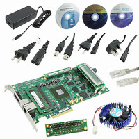
KIT DEV ARRIA II GX FPGA 2AGX125
Manufacturer
Altera
Series
Arria II GXr
Type
FPGAr
Datasheets
1.EP2AGX45CU17C6N.pdf
(96 pages)
2.DK-DEV-2AGX125N.pdf
(48 pages)
3.DK-DEV-2AGX125N.pdf
(64 pages)
Specifications of DK-DEV-2AGX125N
Contents
Board, Cables, CD, DVD, Power Supply
Silicon Manufacturer
Altera
Core Architecture
FPGA
Core Sub-architecture
Arria
Silicon Core Number
EP2
Silicon Family Name
Arria II GX
Rohs Compliant
Yes
For Use With/related Products
EP2AGX125EF35
Lead Free Status / RoHS Status
Lead free / RoHS Compliant
Other names
544-2600
Available stocks
Company
Part Number
Manufacturer
Quantity
Price
Company:

Part Number:
DK-DEV-2AGX125N
Manufacturer:
Altera
Quantity:
135


Chapter 1: Device Datasheet for Arria II Devices
Switching Characteristics
Table 1–44. PLL Specifications for Arria II GX Devices (Part 2 of 3)
December 2010 Altera Corporation
f
f
t
t
t
f
f
t
t
f
t
t
f
t
t
OUT
OUT_EXT
OUTDUTY
OUTPJ_DC
OUTCCJ_DC
OUTPJ_IO
OUTCCJ_IO
CONFIGPLL
CONFIGPHASE
SCANCLK
LOCK
DLOCK
CL B W
PLL_PSERR
ARESET
Symbol
Output frequency for internal global or regional clock
(–4 Speed Grade)
Output frequency for internal global or regional clock
(–5 Speed Grade)
Output frequency for internal global or regional clock
(–6 Speed Grade)
Output frequency for external clock output (–4 Speed Grade)
Output frequency for external clock output (–5 Speed Grade)
Output frequency for external clock output (–6 Speed Grade)
Duty cycle for external clock output (when set to 50%)
Dedicated clock output period jitter (f
Dedicated clock output period jitter (f
Dedicated clock output cycle-to-cycle jitter (f
Dedicated clock output cycle-to-cycle jitter (f
Regular I/O clock output period jitter (f
Regular I/O clock output period jitter (f
Regular I/O clock output cycle-to-cycle jitter (f
Regular I/O clock output cycle-to-cycle jitter (f
Time required to reconfigure PLL scan chains
Time required to reconfigure phase shift
SCANCLK frequency
Time required to lock from end of device configuration
Time required to lock dynamically (after switchover or
reconfiguring any non-post-scale counters/delays)
PLL closed-loop low bandwidth
PLL closed-loop medium bandwidth
PLL closed-loop high bandwidth
Accuracy of PLL phase shift
Minimum pulse width on areset signal
Description
OUT
OUT
OUT
OUT
100 MHz)
100 MHz)
100 MHz)
100 MHz)
OUT
OUT
OUT
OUT
100 MHz)
100 MHz)
100 MHz)
100 MHz)
Arria II Device Handbook Volume 3: Device Datasheet and Addendum
Min
—
—
—
—
—
—
45
—
—
—
—
—
—
—
—
—
—
—
—
—
—
—
—
—
10
Typ
3.5
0.3
1.5
—
—
—
—
—
—
50
—
—
—
—
—
—
—
—
—
—
—
—
—
1
4
670
622
500
Max
500
500
400
300
300
650
650
100
±50
55
30
30
65
65
—
—
—
—
—
—
1
1
(5)
(5)
(5)
mUI (p–p)
mUI (p–p)
mUI (p–p)
mUI (p–p)
SCANCLK
SCANCLK
ps (p–p)
ps (p–p)
ps (p–p)
ps (p–p)
cycles
cycles
Unit
MHz
MHz
MHz
MHz
MHz
MHz
MHz
MHz
MHz
MHz
ms
ms
ps
ns
%
1–59
Related parts for DK-DEV-2AGX125N
Image
Part Number
Description
Manufacturer
Datasheet
Request
R

Part Number:
Description:
KIT DEV CYCLONE III LS EP3CLS200
Manufacturer:
Altera
Datasheet:

Part Number:
Description:
KIT DEV STRATIX IV FPGA 4SE530
Manufacturer:
Altera
Datasheet:

Part Number:
Description:
KIT DEV FPGA 2AGX260 W/6.375G TX
Manufacturer:
Altera
Datasheet:

Part Number:
Description:
KIT DEV MAX V 5M570Z
Manufacturer:
Altera
Datasheet:

Part Number:
Description:
KIT DEV STRATIX V FPGA 5SGXEA7
Manufacturer:
Altera
Datasheet:

Part Number:
Description:
KIT DEVELOPMENT STRATIX III
Manufacturer:
Altera
Datasheet:

Part Number:
Description:
KIT DEVELOPMENT STRATIX IV
Manufacturer:
Altera
Datasheet:

Part Number:
Description:
KIT DEV ARRIA GX 1AGX60N
Manufacturer:
Altera
Datasheet:
Part Number:
Description:
KIT STARTER CYCLONE IV GX
Manufacturer:
Altera
Datasheet:
Part Number:
Description:
KIT DEVELOPMENT STRATIX IV
Manufacturer:
Altera
Datasheet:

Part Number:
Description:
CPLD, EP610 Family, ECMOS Process, 300 Gates, 16 Macro Cells, 16 Reg., 16 User I/Os, 5V Supply, 35 Speed Grade, 24DIP
Manufacturer:
Altera Corporation
Datasheet:
Part Number:
Description:
CPLD, EP610 Family, ECMOS Process, 300 Gates, 16 Macro Cells, 16 Reg., 16 User I/Os, 5V Supply, 15 Speed Grade, 24DIP
Manufacturer:
Altera Corporation
Datasheet: