DK-DEV-3CLS200N Altera, DK-DEV-3CLS200N Datasheet
DK-DEV-3CLS200N
Specifications of DK-DEV-3CLS200N


Related parts for DK-DEV-3CLS200N


DK-DEV-3CLS200N Summary of contents
Page 1
... Innovation Drive San Jose, CA 95134 www.altera.com Cyclone III LS FPGA Development Kit User Guide Document Version: 1.0 Document Date: October 2009 ...
Page 2
... Altera warrants performance of its semiconductor products to current specifications in accordance with Altera's standard warranty, but reserves the right to make changes to any products and services at any time without notice. Altera assumes no responsibility or liability arising out of the application or use of any information, product, or service described herein except as expressly agreed to in writing by Altera Corporation ...
Page 3
... Before You Begin . . . . . . . . . . . . . . . . . . . . . . . . . . . . . . . . . . . . . . . . . . . . . . . . . . . . . . . . . . . . . . . . . . . . . . . . 2–1 Inspect the Board . . . . . . . . . . . . . . . . . . . . . . . . . . . . . . . . . . . . . . . . . . . . . . . . . . . . . . . . . . . . . . . . . . . . . 2–1 References . . . . . . . . . . . . . . . . . . . . . . . . . . . . . . . . . . . . . . . . . . . . . . . . . . . . . . . . . . . . . . . . . . . . . . . . . . . . . . 2–1 Chapter 3. Software Installation Introduction . . . . . . . . . . . . . . . . . . . . . . . . . . . . . . . . . . . . . . . . . . . . . . . . . . . . . . . . . . . . . . . . . . . . . . . . . . . . 3–1 Installing the Altera Complete Design Suite . . . . . . . . . . . . . . . . . . . . . . . . . . . . . . . . . . . . . . . . . . . . . . . . . 3–1 Licensing Considerations . . . . . . . . . . . . . . . . . . . . . . . . . . . . . . . . . . . . . . . . . . . . . . . . . . . . . . . . . . . . . . 3–1 Installing the Cyclone III LS FPGA Development Kit . . . . . . . . . . . . . . . . . . . . . . . . . . . . . . . . . . . . . . . . . 3–2 Installing the USB-Blaster Driver . . . . . . . . . . . . . . . . . . . . . . . . . . . . . . . . . . . . . . . . . . . . . . . . . . . . . . . . . . 3–2 Chapter 4. Development Board Setup Introduction . . . . . . . . . . . . . . . . . . . . . . . . . . . . . . . . . . . . . . . . . . . . . . . . . . . . . . . . . . . . . . . . . . . . . . . . . . . . 4– ...
Page 4
... Programming Flash Memory Using the Nios II EDS . . . . . . . . . . . . . . . . . . . . . . . . . . . . . . . . . . . . . . . . . A–3 Restoring the Flash Device to the Factory Settings . . . . . . . . . . . . . . . . . . . . . . . . . . . . . . . . . . . . . . . . . . A–4 Restoring the MAX II CPLD to the Factory Settings . . . . . . . . . . . . . . . . . . . . . . . . . . . . . . . . . . . . . . . . . A–5 Additional Information Revision History . . . . . . . . . . . . . . . . . . . . . . . . . . . . . . . . . . . . . . . . . . . . . . . . . . . . . . . . . . . . . . . . . . . . . Info–1 How to Contact Altera . . . . . . . . . . . . . . . . . . . . . . . . . . . . . . . . . . . . . . . . . . . . . . . . . . . . . . . . . . . . . . . . Info–1 Cyclone III LS FPGA Development Kit User Guide October 2009 Altera Corporation ...
Page 5
... Typographic Conventions . . . . . . . . . . . . . . . . . . . . . . . . . . . . . . . . . . . . . . . . . . . . . . . . . . . . . . . . . . . . . Info–1 October 2009 Altera Corporation Cyclone III LS FPGA Development Kit User Guide v ...
Page 6
... Cyclone III LS FPGA Development Kit User Guide October 2009 Altera Corporation ...
Page 7
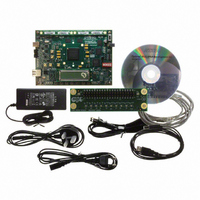
... USB cable Ethernet cable Software Altera Complete Design Suite DVD—A DVD that includes the following items: Quartus II Software—The Quartus II software, including the SOPC Builder system development tool, provides a comprehensive environment for system-on-a-programmable-chip (SOPC) design. The Quartus II software integrates into nearly any design environment and provides interfaces to industry-standard EDA tools ...
Page 8
... The kit includes a development kit edition (DKE) license for the Quartus II software (Windows platform only). This license entitles you to all the features of the subscription edition for a period of one year. After the year, you must purchase a renewal subscription to continue using the software. ...
Page 9
... For more information about power consumption and thermal modeling, refer to AN 358: Thermal Management for References Use the following links to check the Altera website for the following other related information: © October 2009 Altera Corporation 2. Getting Started Manual. ...
Page 10
... For Nios II 32-bit embedded processor solutions, refer to the Processing Cyclone III LS FPGA Development Kit User Guide page. page. page. Chapter 2: Getting Started References Cyclone III LS Development Literature: Cyclone III Devices page. Capture CIS Symbols page. Embedded © October 2009 Altera Corporation ...
Page 11
... Suite DVD are the Quartus II software and the Nios II EDS. The Quartus II software (including SOPC Builder) and the Nios II EDS are the primary FPGA development tools used to create the reference designs in this development kit. To install the Altera software tools, perform the following steps: 1 ...
Page 12
... Installation instructions for the USB-Blaster driver for your operating system are available on the Altera website. On the page of the Altera website, locate the table entry for your configuration and click the link to access the instructions. Cyclone III LS FPGA Development Kit User Guide ...
Page 13
... Quartus II software INIT_DONE option on, the FPGA INIT DONE LED (D14) illuminates when the device enters user mode. f For more information about the PFL megafunction, refer to Flash Loader with the Quartus II © October 2009 Altera Corporation 4. Development Board Setup “Factory Default Switch Settings” on page 4–2 AN 386: Using the Parallel Software. ...
Page 14
... Position Off On Off Off Chapter 4: Development Board Setup Factory Default Switch Settings JTAG Control Jumpers J11 (installed) (not installed) (not installed) J12 (not installed) Board Settings DIP Switch OPEN OFF = SW2 Figure 4–1. Figure 4–1. © October 2009 Altera Corporation ...
Page 15
... J11 pins 1-2 J11 pins 3-4 J11 pins 5-6 J12 J18 f For more information about the FPGA board settings, refer to the Development Board Reference © October 2009 Altera Corporation Table 4–3 and Figure Shunt Position Installed Not Installed Not Installed Not Installed Not Installed Manual ...
Page 16
... Cyclone III LS FPGA Development Kit User Guide Chapter 4: Development Board Setup Factory Default Switch Settings © October 2009 Altera Corporation ...
Page 17
... The design can obtain an IP address from any DHCP server and serve a web page from the flash on your board to any host computer on the same network. The web page allows you to upload new FPGA designs to the user portion of flash memory, and provides links to useful information on the Altera website, including links to kit-specific and design resources. 1 After successfully updating the flash memory user design, you can load the user design from flash memory into the FPGA ...
Page 18
... Board Update Portal web page the Hardware File Name field specify the .flash file that you either downloaded from the Altera website or created on your own. If there is a software component to the design, specify it in the same manner using the Software File Name field, otherwise leave the Software File Name field blank ...
Page 19
... A GUI runs on the PC which communicates over the JTAG bus to a test design running in the Cyclone III LS device the factory configuration. © October 2009 Altera Corporation 6. Board Test System 3–2. Figure 6–1 shows the initial GUI for a board that ...
Page 20
... JTAG bus, other applications using the JTAG bus might time out. Be sure to close the other applications before attempting to reconfigure the FPGA using the Quartus II Programmer. Cyclone III LS FPGA Development Kit User Guide Chapter 6: Board Test System Introduction ® II Embedded Logic © October 2009 Altera Corporation ...
Page 21
... BoardTestSystem.exe application Windows, click Start > All Programs > Altera > Cyclone III LS FPGA Development Kit <version> > Board Test System to run the application. A GUI appears, displaying the application tab that corresponds to the design running in the FPGA. The Cyclone III LS FPGA development board’s flash memory ships preconfigured with the design that corresponds to the Config, GPIO, and SRAM& ...
Page 22
... Cyclone III LS FPGA Development Kit User Guide shows the Config tab. The tab displays the contents of the 6–1. Changes to the register values with the GUI take effect Chapter 6: Board Test System Using the Board Test System © October 2009 Altera Corporation ...
Page 23
... MAX II register values. Refer to 1 Because the Config tab requires that a specific design is running in the FPGA, writing SRST or changing the PSO value can cause the Board Test System to stop running. © October 2009 Altera Corporation Read/Write Capability Write only Set initiate an FPGA reconfiguration. ...
Page 24
... LEDs on or off, and detect push button presses. Cyclone III LS FPGA Development Kit User Guide Chapter 6: Board Test System Using the Board Test System Cyclone III LS FPGA Development Kit Figure 6–3 shows the GPIO tab. © October 2009 Altera Corporation page of ...
Page 25
... Change the switches on the board to see the graphical display change accordingly. User LEDs This control displays the current state of the user LEDs. Click on the graphical representation of the LEDs to turn the board LEDs on and off. © October 2009 Altera Corporation 6–7 Cyclone III LS FPGA Development Kit User Guide ...
Page 26
... SRAM in this Nios II-based BTS design is 0x0D00.0000. The valid address range within the 2-MByte SRAM is 0x0000.0000 through 0x001F.FFFF, as shown in the GUI. Cyclone III LS FPGA Development Kit User Guide shows the SRAM&Flash tab. Chapter 6: Board Test System Using the Board Test System © October 2009 Altera Corporation ...
Page 27
... The DDR2 Tab The DDR2 tab allows you to read and write the DDR2 memory on your board. Figure 6–5 shows the DDR2 tab. © October 2009 Altera Corporation Table A–1 on page A–1). 6–9 Figure 6–1 on Cyclone III LS FPGA Development Kit User Guide ...
Page 28
... Write, Read, and Total performance bars—Show the percentage of maximum data rate that the requested transactions are able to achieve. Cyclone III LS FPGA Development Kit User Guide Chapter 6: Board Test System Using the Board Test System © October 2009 Altera Corporation ...
Page 29
... Write Only—Selects write transactions for analysis. The HSMC Tab The HSMC tab allows you to perform loopback tests on the HSMC A and HSMC B ports. Figure 6–6 © October 2009 Altera Corporation shows the HSMC tab. Cyclone III LS FPGA Development Kit User Guide 6–11 ...
Page 30
... Port This control allows you to specify the type of test to run on the HSMC ports. The following HSMC port tests are available: Cyclone III LS FPGA Development Kit User Guide Chapter 6: Board Test System Using the Board Test System © October 2009 Altera Corporation ...
Page 31
... The Power Monitor The Power Monitor measures and reports current power information for the board. To start the application, click Power Monitor in the Board Test System application. © October 2009 Altera Corporation 6–13 Cyclone III LS FPGA Development Kit User Guide ...
Page 32
... You can also run the Power Monitor as a stand-alone application. PowerTool.exe resides in the <install dir>\kits\cycloneIIILS_3cls200_fpga\examples\board_test_system directory. On Windows, click Start > All Programs > Altera > Cyclone III LS FPGA Development Kit <version> > Power Monitor to start the application. The Power Monitor communicates to the MAX II device on the board through the JTAG bus ...
Page 33
... The first measurement is Vsense and the difference between the two measurements is Vdif. Plug the values into the equation to determine the power consumption. © October 2009 Altera Corporation Cyclone III LS FPGA Manual. Cyclone III LS FPGA Development Kit User Guide ...
Page 34
... Turn on the Program/Configure option for the added file. 4. Click Start to download the selected file to the FPGA. Configuration is complete when the progress bar reaches 100%. Cyclone III LS FPGA Development Kit User Guide Chapter 6: Board Test System Configuring the FPGA Using the Quartus II Programmer © October 2009 Altera Corporation ...
Page 35
... Introduction As you develop your own project using the Altera tools, you can program the flash memory device so that your own design loads from flash memory into the FPGA on power up. This appendix describes the preprogrammed contents of the common flash interface (CFI) flash memory device on the Cyclone III LS FPGA development board and the Nios II EDS tools involved with reprogramming the user portions of the flash memory device ...
Page 36
... If you have an FPGA design developed using the Quartus II software, and software developed using the Nios II EDS, follow these instructions the Windows Start menu, click All Programs > Altera > Nios II EDS > Nios II Command Shell the Nios II command shell, navigate to the directory where your design files reside and type the following Nios II EDS commands: For Quartus II ...
Page 37
... The CONF DONE LED (D14) and the four user LEDs (D25-D28) illuminate indicating that the flash device is ready for programming the Windows Start menu, click All Programs > Altera > Nios II EDS > Nios II Command Shell the Nios II command shell, navigate to the <install dir> ...
Page 38
... The CONF DONE LED (D14) and the four user LEDs (D25-D28) illuminate indicating that the flash device is ready for programming the Windows Start menu, click All Programs > Altera > Nios II EDS > Nios II Command Shell the Nios II command shell, navigate to the <install dir> ...
Page 39
... To ensure that you have the most up-to-date factory restore files and information about this product, refer to the Altera website. © October 2009 Altera Corporation Altera Development Kits page on the Altera website. 4–2. Cyclone III LS FPGA Development Kit Cyclone III LS FPGA Development Kit User Guide A–5 “ ...
Page 40
... A–6 Cyclone III LS FPGA Development Kit User Guide Appendix A: Programming the Flash Memory Device Restoring the MAX II CPLD to the Factory Settings © October 2009 Altera Corporation ...
Page 41
... Product literature Non-technical support (General) Email (Software Licensing) Email Note to Table: (1) You can also contact your local Altera sales office or sales representative. Typographic Conventions This document uses the typographic conventions shown in the following table. Visual Cue Bold Type with Initial Capital ...
Page 42
... A warning calls attention to a condition or possible situation that can cause you injury. The angled arrow instructs you to press Enter. The feet direct you to more information about a particular topic. Additional Information Typographic Conventions © October 2009 Altera Corporation ...