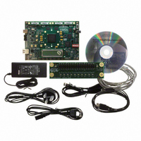
DK-DEV-3CLS200N Altera, DK-DEV-3CLS200N Datasheet - Page 24

DK-DEV-3CLS200N
Manufacturer Part Number
DK-DEV-3CLS200N
Description
KIT DEV CYCLONE III LS EP3CLS200
Manufacturer
Altera
Series
Cyclone® IIIr
Type
FPGAr
Datasheets
1.EP3C5F256C8N.pdf
(34 pages)
2.EP3C5F256C8N.pdf
(14 pages)
3.DK-START-3C25N.pdf
(74 pages)
4.DK-DEV-3CLS200N.pdf
(42 pages)
Specifications of DK-DEV-3CLS200N
Contents
Board
Silicon Manufacturer
Altera
Core Architecture
FPGA
Core Sub-architecture
Cyclone
Silicon Core Number
EP3C
Silicon Family Name
Cyclone III LS
Rohs Compliant
Yes
For Use With/related Products
EP3CLS200
Lead Free Status / RoHS Status
Lead free / RoHS Compliant
Other names
544-2601
6–6
The GPIO Tab
Cyclone III LS FPGA Development Kit User Guide
1
JTAG Chain
This control shows all the devices currently in the JTAG chain. The Cyclone III LS
device is always the first device in the chain.
Installing the shunt jumper on jumper J11 pins 1-2 includes the MAX II device in the
JTAG chain. Installing the shunt jumper on jumper J12 or setting the anti-tamper DIP
switch SW2.3 to the off position breaks the JTAG chain.
Board Information
Flash Memory Map
This control shows the memory map of the flash memory device on your board.
The GPIO tab allows you to interact with all the general purpose user I/O
components on your board. You can write to the LCD, read DIP switch settings, turn
LEDs on or off, and detect push button presses.
f
MAX-II rev—Indicates the version of MAX II code currently running on the
board. The MAX II code resides in the <install
dir>\kits\cycloneIIILS_3cls200_fpga\examples directory. Newer revisions of
this code might be available on the
the Altera website.
MAC—Indicates the MAC address of the board.
For information about the anti-tamper design example, refer to <install
dir>\kits\cycloneIIILS_3cls200_fpga\examples\max2\at_example\rea
dme_at_example.txt.
Cyclone III LS FPGA Development Kit
Figure 6–3
shows the GPIO tab.
© October 2009 Altera Corporation
Chapter 6: Board Test System
Using the Board Test System
page of


