DK-DEV-3CLS200N Altera, DK-DEV-3CLS200N Datasheet - Page 20
DK-DEV-3CLS200N
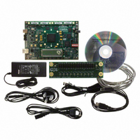
Manufacturer Part Number
DK-DEV-3CLS200N
Description
KIT DEV CYCLONE III LS EP3CLS200
Manufacturer
Altera
Series
Cyclone® IIIr
Type
FPGAr
Datasheets
1.EP3C5F256C8N.pdf
(34 pages)
2.EP3C5F256C8N.pdf
(14 pages)
3.DK-START-3C25N.pdf
(74 pages)
4.DK-DEV-3CLS200N.pdf
(42 pages)
Specifications of DK-DEV-3CLS200N
Contents
Board
Silicon Manufacturer
Altera
Core Architecture
FPGA
Core Sub-architecture
Cyclone
Silicon Core Number
EP3C
Silicon Family Name
Cyclone III LS
Rohs Compliant
Yes
For Use With/related Products
EP3CLS200
Lead Free Status / RoHS Status
Lead free / RoHS Compliant
Other names
544-2601


6–2
Figure 6–1. Board Test System Graphical User Interface
Cyclone III LS FPGA Development Kit User Guide
1
Several designs are provided to test the major board features. Each design provides
data for one or more tabs in the application. The Configure menu identifies the
appropriate design to download to the FPGA for each tab.
After successful FPGA configuration, the appropriate tab appears and allows you to
exercise the related board features. Highlights appear in the board picture around the
corresponding components.
The Power Monitor button starts the Power Monitor application that measures and
reports current power information for the board. Because the application
communicates over the JTAG bus to the MAX II device, you can measure the power of
any design in the FPGA, including your own designs.
The Board Test System and Power Monitor share the JTAG bus with other
applications like the Nios II debugger and the SignalTap
Analyzer. Because the Quartus II programmer uses most of the bandwidth of the
JTAG bus, other applications using the JTAG bus might time out. Be sure to close the
other applications before attempting to reconfigure the FPGA using the Quartus II
Programmer.
®
II Embedded Logic
© October 2009 Altera Corporation
Chapter 6: Board Test System
Introduction
Related parts for DK-DEV-3CLS200N
Image
Part Number
Description
Manufacturer
Datasheet
Request
R

Part Number:
Description:
KIT DEV ARRIA II GX FPGA 2AGX125
Manufacturer:
Altera
Datasheet:

Part Number:
Description:
KIT DEV STRATIX IV FPGA 4SE530
Manufacturer:
Altera
Datasheet:

Part Number:
Description:
KIT DEV FPGA 2AGX260 W/6.375G TX
Manufacturer:
Altera
Datasheet:

Part Number:
Description:
KIT DEV MAX V 5M570Z
Manufacturer:
Altera
Datasheet:

Part Number:
Description:
KIT DEV STRATIX V FPGA 5SGXEA7
Manufacturer:
Altera
Datasheet:

Part Number:
Description:
KIT DEVELOPMENT STRATIX III
Manufacturer:
Altera
Datasheet:

Part Number:
Description:
KIT DEVELOPMENT STRATIX IV
Manufacturer:
Altera
Datasheet:

Part Number:
Description:
KIT DEV ARRIA GX 1AGX60N
Manufacturer:
Altera
Datasheet:
Part Number:
Description:
KIT STARTER CYCLONE IV GX
Manufacturer:
Altera
Datasheet:
Part Number:
Description:
KIT DEVELOPMENT STRATIX IV
Manufacturer:
Altera
Datasheet:

Part Number:
Description:
CPLD, EP610 Family, ECMOS Process, 300 Gates, 16 Macro Cells, 16 Reg., 16 User I/Os, 5V Supply, 35 Speed Grade, 24DIP
Manufacturer:
Altera Corporation
Datasheet:
Part Number:
Description:
CPLD, EP610 Family, ECMOS Process, 300 Gates, 16 Macro Cells, 16 Reg., 16 User I/Os, 5V Supply, 15 Speed Grade, 24DIP
Manufacturer:
Altera Corporation
Datasheet: