DK-DEV-4SGX230N Altera, DK-DEV-4SGX230N Datasheet - Page 13
DK-DEV-4SGX230N
Manufacturer Part Number
DK-DEV-4SGX230N
Description
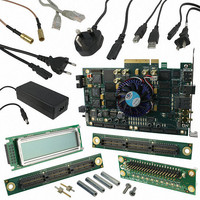
KIT DEVELOPMENT STRATIX IV
Manufacturer
Altera
Series
Stratix® IVr
Type
FPGAr
Datasheets
1.EP4SGX110DF29C3N.pdf
(80 pages)
2.EP4SGX110DF29C3N.pdf
(1154 pages)
3.DK-DEV-4SGX230N.pdf
(2 pages)
4.DK-DEV-4SGX530N.pdf
(57 pages)
Specifications of DK-DEV-4SGX230N
Contents
Development Board, Universal Power Supply, Cables and Software
Silicon Manufacturer
Altera
Core Architecture
FPGA
Core Sub-architecture
Stratix
Silicon Core Number
EP4S
Silicon Family Name
Stratix IV GX
Rohs Compliant
Yes
For Use With/related Products
EP4SGX230K
Lead Free Status / RoHS Status
Lead free / RoHS Compliant
Other names
544-2594
Available stocks
Company
Part Number
Manufacturer
Quantity
Price
Company:

Part Number:
DK-DEV-4SGX230N
Manufacturer:
Altera
Quantity:
135


Chapter 1: DC and Switching Characteristics for Stratix IV Devices
Electrical Characteristics
Table 1–6. Transceiver Power Supply Operating Conditions for Stratix IV GX Devices
Table 1–7. Transceiver Power Supply Operating Conditions for Stratix IV GT Devices (Part 1 of 2)
April 2011 Altera Corporation
V
V
V
V
V
V
V
V
V
V
V
V
Notes to
(1) Transceiver power supplies do not have power-on-reset (POR) circuitry. After initial power-up, violating the transceiver power supply operating
(2) V
(3) n = 0, 1, 2, or 3.
(4) V
V
V
V
V
V
V
V
V
V
V
V
CCA_L
CCA_R
CCHIP_L
CCHIP_R
CCR_L
CCR_R
CCT_L
CCT_R
CCL_GXBLn
CCL_GXBRn
CCH_GXBLn
CCH_GXBRn
CCA_L
CCA_R
CCHIP_L
CCHIP_R
CCR_L
CCR_R
CCT_L
CCT_R
CCL_GXBLn
CCL_GXBRn
CCH_GXBLn
conditions could lead to unpredictable link behavior.
or both, are configured at a base data rate > 4.25 Gbps. For data rates up to 4.25 Gbps, you can connect V
connect V
CCA_L/R
CCH_GXBL/R
Symbol
Symbol
Table
(3)
(3)
must be connected to a 3.0-V supply if the clock multiplier unit (CMU) phase-locked loop (PLL), receiver clock data recovery (CDR),
(3)
(3)
(3)
(3)
(3)
CCH_GXBL/R
1–6:
must be connected to a 1.4-V supply if the transmitter channel data rate is > 6.5 Gbps. For data rates up to 6.5 Gbps, you can
Transceiver high voltage power (left side)
Transceiver high voltage power (right side)
Transceiver HIP digital power (left side)
Transceiver HIP digital power (right side)
Receiver power (left side)
Receiver power (right side)
Transmitter power (left side)
Transmitter power (right side)
Transceiver clock power (right side)
Transmitter output buffer power (left side)
Transceiver clock power (left side)
Transmitter output buffer power (right side)
Transceiver clock power (left side)
to either 1.4 V or 1.5 V.
Table 1–6
Stratix IV GX devices.
Table 1–7
transceiver power supply.
lists the transceiver power supply recommended operating conditions for
lists the recommended operating conditions for the Stratix IV GT
Description
Description
Stratix IV Device Handbook Volume 4: Device Datasheet and Addendum
2.85/2.375
1.33/1.425
Minimum
Minimum
1.045
1.045
1.045
1.045
3.17
3.17
0.92
0.92
1.15
1.15
1.15
1.15
1.15
1.15
1.33
0.87
0.87
1.05
1.05
(Note 1)
3.0/2.5
1.4/1.5
Typical
Typical
0.95
0.95
0.9
0.9
1.1
1.1
1.1
1.1
1.1
1.1
CCA_L/R
3.3
3.3
1.2
1.2
1.2
1.2
1.2
1.2
1.4
(2)
(4)
to either 3.0 V or 2.5 V.
(Note
3.15/2.625
1.47/1.575
Maximum
Maximum
1.155
1.155
1.155
1.155
0.93
0.93
1.15
1.15
3.43
3.43
0.98
0.98
1.25
1.25
1.25
1.25
1.25
1.25
1.47
1),
(2)
Unit
Unit
V
V
V
V
V
V
V
V
V
V
V
V
V
V
V
V
V
V
V
V
V
1–5
Related parts for DK-DEV-4SGX230N
Image
Part Number
Description
Manufacturer
Datasheet
Request
R

Part Number:
Description:
KIT DEV ARRIA II GX FPGA 2AGX125
Manufacturer:
Altera
Datasheet:

Part Number:
Description:
KIT DEV CYCLONE III LS EP3CLS200
Manufacturer:
Altera
Datasheet:

Part Number:
Description:
KIT DEV STRATIX IV FPGA 4SE530
Manufacturer:
Altera
Datasheet:

Part Number:
Description:
KIT DEV FPGA 2AGX260 W/6.375G TX
Manufacturer:
Altera
Datasheet:

Part Number:
Description:
KIT DEV MAX V 5M570Z
Manufacturer:
Altera
Datasheet:

Part Number:
Description:
KIT DEV STRATIX V FPGA 5SGXEA7
Manufacturer:
Altera
Datasheet:

Part Number:
Description:
KIT DEVELOPMENT STRATIX III
Manufacturer:
Altera
Datasheet:

Part Number:
Description:
KIT DEV ARRIA GX 1AGX60N
Manufacturer:
Altera
Datasheet:
Part Number:
Description:
KIT STARTER CYCLONE IV GX
Manufacturer:
Altera
Datasheet:
Part Number:
Description:
KIT DEVELOPMENT STRATIX IV
Manufacturer:
Altera
Datasheet:

Part Number:
Description:
CPLD, EP610 Family, ECMOS Process, 300 Gates, 16 Macro Cells, 16 Reg., 16 User I/Os, 5V Supply, 35 Speed Grade, 24DIP
Manufacturer:
Altera Corporation
Datasheet:
Part Number:
Description:
CPLD, EP610 Family, ECMOS Process, 300 Gates, 16 Macro Cells, 16 Reg., 16 User I/Os, 5V Supply, 15 Speed Grade, 24DIP
Manufacturer:
Altera Corporation
Datasheet: