EVAL-ADUC832QSZ Analog Devices Inc, EVAL-ADUC832QSZ Datasheet - Page 20
EVAL-ADUC832QSZ
Manufacturer Part Number
EVAL-ADUC832QSZ
Description
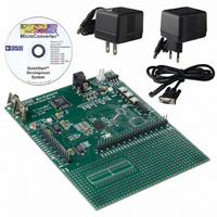
KIT DEV FOR ADUC832 QUICK START
Manufacturer
Analog Devices Inc
Series
QuickStart™ Kitr
Type
MCUr
Specifications of EVAL-ADUC832QSZ
Contents
Evaluation Board, Cable, Power Supply, Software and Documentation
Lead Free Status / RoHS Status
Lead free / RoHS Compliant
For Use With/related Products
ADuC832
Lead Free Status / RoHS Status
Compliant, Lead free / RoHS Compliant
Other names
EVAL-ADUC832QS
EVAL-ADUC832QS
EVAL-ADUC832QS


ADuC832
ADCCON2 – (ADC Control SFR #2)
The ADCCON2 register controls ADC channel selection and
conversion modes as detailed below.
SFR Address:
SFR Power-On Default Value:
Bit Addressable:
Bit
ADCCON2.7 ADCI
ADCCON2.6 DMA
ADCCON2.5 CCONV
ADCCON2.4 SCONV
ADCCON2.3 CS3
ADCCON2.2 CS2
ADCCON2.1 CS1
ADCCON2.0 CS0
Name
Description
The ADC interrupt bit (ADCI) is set by hardware at the end of a single ADC conversion cycle or at
the end of a DMA block conversion. ADCI is cleared by hardware when the PC vectors to the ADC
Interrupt Service Routine. Otherwise, the ADCI bit should be cleared by user code.
The DMA mode enable bit (DMA) is set by the user to enable a preconfigured ADC DMA mode opera-
tion. A more detailed description of this mode is given in the ADC DMA Mode section. The DMA bit is
automatically set to “0” at the end of a DMA cycle. Setting this bit causes the ALE output to cease, it will
start again when DMA is started and will operate correctly after DMA is complete.
The continuous conversion bit (CCONV) is set by the user to initiate the ADC into a continuous mode of
conversion. In this mode, the ADC starts converting based on the timing and channel configuration
already set up in the ADCCON SFRs; the ADC automatically starts another conversion once a previ-
ous conversion has completed.
The single conversion bit (SCONV) is set to initiate a single conversion cycle. The SCONV bit is
automatically reset to “0” on completion of the single conversion cycle.
The channel selection bits (CS3–0) allow the user to program the ADC channel selection under
software control. When a conversion is initiated, the channel converted will be that pointed to by
these channel selection bits. In DMA mode, the channel selection is derived from the channel ID
written to the external memory.
CS3 CS2 CS1 CS0 CH#
0
0
0
0
0
0
0
0
1
1
1
1
1
1
All other combinations reserved
D8H
00H
YES
0
0
0
0
1
1
1
1
0
0
0
0
1
1
0
0
1
1
0
0
1
1
0
0
1
1
0
1
Table IV. ADCCON2 SFR Bit Designations
0
1
0
1
0
1
0
1
0
1
0
1
0
1
0
1
2
3
4
5
6
7
Temp Monitor
DAC0
DAC1
AGND
VREF
DMA STOP
–20–
Only use with Internal DAC o/p buffer on
Only use with Internal DAC o/p buffer on
Place in XRAM location to finish DMA sequence, see
Requires minimum of 1 µs to acquire
the section ADC DMA Mode.
REV. 0
Related parts for EVAL-ADUC832QSZ
Image
Part Number
Description
Manufacturer
Datasheet
Request
R


Part Number:
Description:
BOARD EVAL FOR SI270X-A
Manufacturer:
Silicon Laboratories Inc
Datasheet:

Part Number:
Description:
BUCK CONV REF DESIGN KIT IP1201
Manufacturer:
International Rectifier
Datasheet:
Part Number:
Description:
BOARD DEMO SYNC DUAL BUCK CNVTER
Manufacturer:
International Rectifier
Datasheet:
Part Number:
Description:
BOARD DEMO SYNC BUCK CONVETER
Manufacturer:
International Rectifier
Datasheet:

Part Number:
Description:
EVALBOARD/EB Omnidirectional microphone - Analog
Manufacturer:
Analog Devices
Datasheet:
Part Number:
Description:
EVALBOARD/EB Omnidirectional microphone - Analog
Manufacturer:
Analog Devices
Datasheet:


Part Number:
Description:
BOARD EVAL LED DRIVER LT3756
Manufacturer:
Linear Technology
Datasheet:

Part Number:
Description:
BOARD EVAL FOR AD7741/7742
Manufacturer:
Analog Devices Inc
Datasheet:

Part Number:
Description:
±1.7g Dual-Axis IMEMS Accelerometer Evaluation Board
Manufacturer:
Analog Devices Inc
Datasheet:

Part Number:
Description:
IC MULTIPLIER ANALOG 8-SOIC T/R
Manufacturer:
Analog Devices Inc
Datasheet:

Part Number:
Description:
IC ANALOG MULTIPLIER 8-DIP
Manufacturer:
Analog Devices Inc
Datasheet:
Part Number:
Description:
IC ANALOG MULTIPLIER 8-SOIC
Manufacturer:
Analog Devices Inc
Datasheet:
Part Number:
Description:
IC ANALOG MULTIPLIER 8-DIP
Manufacturer:
Analog Devices Inc
Datasheet: