EVAL-ADUC832QSZ Analog Devices Inc, EVAL-ADUC832QSZ Datasheet - Page 4
EVAL-ADUC832QSZ
Manufacturer Part Number
EVAL-ADUC832QSZ
Description
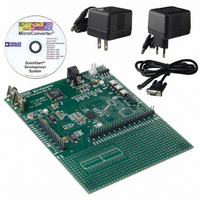
KIT DEV FOR ADUC832 QUICK START
Manufacturer
Analog Devices Inc
Series
QuickStart™ Kitr
Type
MCUr
Specifications of EVAL-ADUC832QSZ
Contents
Evaluation Board, Cable, Power Supply, Software and Documentation
Lead Free Status / RoHS Status
Lead free / RoHS Compliant
For Use With/related Products
ADuC832
Lead Free Status / RoHS Status
Compliant, Lead free / RoHS Compliant
Other names
EVAL-ADUC832QS
EVAL-ADUC832QS
EVAL-ADUC832QS


ADuC832
SPECIFICATIONS
Parameter
DAC CHANNEL SPECIFICATIONS
DC ACCURACY
ANALOG OUTPUTS
REFERENCE INPUT/OUTPUT
EXTERNAL REFERENCE INPUT
POWER SUPPLY MONITOR (PSM)
WATCHDOG TIMER (WDT)
FLASH/EE MEMORY RELIABILITY
CHARACTERISTICS
DIGITAL INPUTS
Internal Buffer Disabled
Resolution
Relative Accuracy
Differential Nonlinearity
Offset Error
Gain Error
Gain Error Mismatch
Voltage Range_0
REFERENCE OUTPUT
Output Voltage (V
Accuracy
Power Supply Rejection
Reference Temperature Coefficient
Internal V
Voltage Range (V
Input Impedance
Input Leakage
DV
DV
Timeout Period
Endurance
Data Retention
Input High Voltage (V
Input Low Voltage (V
Input Leakage Current (Port 0, EA)
Logic 1 Input Current
Logic 0 Input Current (Port 1, 2, 3)
Logic 1–0 Transition Current (Port 2, 3)
(All Digital Inputs)
DD
DD
Trip Point Selection Range
Power Supply Trip Point Accuracy
REF
17
Power-On Time
18
10
REF
REF
)
16
4
4
)
INL
INH
(continued)
11
)
)
14
4
4
4
15
12, 13
V
12
± 3
–1
± 1/2
± 5
–0.3
0.5
0 to V
2.5
± 2.5
47
± 100
80
0.1
V
20
1
2.63
4.37
± 3.5
0
2000
100,000
100
2.4
0.8
± 10
± 1
± 10
± 1
–75
–40
–660
–400
DD
DD
= 5 V
REF
V
12
± 3
–1
± 1/2
± 5
–0.3
0.5
0 to V
2.5
± 2.5
57
± 100
80
0.1
V
20
1
0
2000
100,000
100
2
0.4
± 10
± 1
± 10
± 1
–25
–15
–250
–140
–4–
DD
DD
= 3 V
REF
Unit
Bits
LSB typ
LSB max
LSB typ
mV max
% typ
% max
V typ
V
% max
dB typ
ppm/°C typ
ms typ
V min
V max
kΩ typ
µA max
V min
V max
% max
ms min
ms max
Cycles min
Years min
V min
V max
µA max
µA typ
µA max
µA typ
µA max
µA typ
µA max
µA typ
Test Conditions/Comments
Guaranteed 12-Bit Monotonic
V
V
% of Full-Scale on DAC1
DAC V
Of V
V
Internal Band Gap Deselected via
ADCCON1.6
Four Trip Points Selectable in
This Range Programmed via
TPD1–0 in PSMCON
Nine Timeout Periods
Selectable in this Range
V
V
V
V
V
V
V
REF
REF
REF
IN
IN
IN
IN
IL
IL
IL
= 450 mV
= 2 V
= 2 V
= 0 V or V
= 0 V or V
= V
= V
REF
Range
Range
and C
REF
DD
DD
Measured at the C
= 2.5 V
REF
DD
DD
Pins Shorted
REF
REV. 0
Pin
Related parts for EVAL-ADUC832QSZ
Image
Part Number
Description
Manufacturer
Datasheet
Request
R


Part Number:
Description:
BOARD EVAL FOR SI270X-A
Manufacturer:
Silicon Laboratories Inc
Datasheet:

Part Number:
Description:
BUCK CONV REF DESIGN KIT IP1201
Manufacturer:
International Rectifier
Datasheet:
Part Number:
Description:
BOARD DEMO SYNC DUAL BUCK CNVTER
Manufacturer:
International Rectifier
Datasheet:
Part Number:
Description:
BOARD DEMO SYNC BUCK CONVETER
Manufacturer:
International Rectifier
Datasheet:

Part Number:
Description:
EVALBOARD/EB Omnidirectional microphone - Analog
Manufacturer:
Analog Devices
Datasheet:
Part Number:
Description:
EVALBOARD/EB Omnidirectional microphone - Analog
Manufacturer:
Analog Devices
Datasheet:


Part Number:
Description:
BOARD EVAL LED DRIVER LT3756
Manufacturer:
Linear Technology
Datasheet:

Part Number:
Description:
BOARD EVAL FOR AD7741/7742
Manufacturer:
Analog Devices Inc
Datasheet:

Part Number:
Description:
±1.7g Dual-Axis IMEMS Accelerometer Evaluation Board
Manufacturer:
Analog Devices Inc
Datasheet:

Part Number:
Description:
IC MULTIPLIER ANALOG 8-SOIC T/R
Manufacturer:
Analog Devices Inc
Datasheet:

Part Number:
Description:
IC ANALOG MULTIPLIER 8-DIP
Manufacturer:
Analog Devices Inc
Datasheet:
Part Number:
Description:
IC ANALOG MULTIPLIER 8-SOIC
Manufacturer:
Analog Devices Inc
Datasheet:
Part Number:
Description:
IC ANALOG MULTIPLIER 8-DIP
Manufacturer:
Analog Devices Inc
Datasheet: