EVAL-ADUC832QSZ Analog Devices Inc, EVAL-ADUC832QSZ Datasheet - Page 30
EVAL-ADUC832QSZ
Manufacturer Part Number
EVAL-ADUC832QSZ
Description
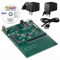
KIT DEV FOR ADUC832 QUICK START
Manufacturer
Analog Devices Inc
Series
QuickStart™ Kitr
Type
MCUr
Specifications of EVAL-ADUC832QSZ
Contents
Evaluation Board, Cable, Power Supply, Software and Documentation
Lead Free Status / RoHS Status
Lead free / RoHS Compliant
For Use With/related Products
ADuC832
Lead Free Status / RoHS Status
Compliant, Lead free / RoHS Compliant
Other names
EVAL-ADUC832QS
EVAL-ADUC832QS
EVAL-ADUC832QS


ADuC832
Example: Programming the Flash/EE Data Memory
A user wishes to program F3H into the second byte on Page
03H of the Flash/EE data memory space while preserving the
other three bytes already in this page.
A typical program of the Flash/EE Data array will involve:
Step 1: Set Up the Page Address
The two address registers EADRH and EADRL hold the high
byte address and the low byte address of the page to be addressed.
The assembly language to set up the address may appear as:
Step 2: Set Up the EDATA Registers
We must now write the four values to be written into the page
into the four SFRs EDATA1–4. Unfortunately, we do not know
three of them. Thus, we must read the current page and over-
write the second byte.
Step 3: Program Page
A byte in the Flash/EE array can only be programmed if it has
previously been erased. To be more specific, a byte can only be
programmed if it already holds the value FFH. Because of the
Flash/EE architecture, this erase must happen at a page level;
therefore, a minimum of four bytes (one page) will be erased
when an erase command is initiated. Once the page is erased we
can program the four bytes in-page and then perform a verification
of the data.
Although the 4 kBytes of Flash/EE data memory are shipped
from the factory pre-erased, i.e., byte locations set to FFH, it is
nonetheless good programming practice to include an erase-all
routine as part of any configuration/setup code running on the
ADuC832. An ERASE-ALL command consists of writing
“06H” to the ECON SFR, which initiates an erase of the 4 kByte
Flash/EE array. This command coded in 8051 assembly would
appear as:
MOV EADRH,#0
MOV EADRL,#03H
MOV
MOV
MOV
MOV
MOV
MOV
JNZ
MOV
1) setting EADRH/L with the page address
2) writing the data to be programmed to the EDATA1–4
3) writing the ECON SFR with the appropriate command
ECON,#1
EDATA2,#0F3H ; Overwrite byte 2
ECON,#5
ECON,#2
ECON,#4
A,ECON
ERROR
ECON,#06H
; Set Page Address Pointer
; Read Page into EDATA1-4
; ERASE Page
; WRITE Page
; VERIFY Page
; Check if ECON=0 (OK!)
; Erase all Command
; 2 ms Duration
–30–
Flash/EE Memory Timing
Typical program and erase times for the ADuC832 are as follows:
NORMAL MODE (operating on Flash/EE data memory)
ULOAD MODE (operating on Flash/EE program memory)
It should be noted that a given mode of operation is initiated as
soon as the command word is written to the ECON SFR. The
core microcontroller operation on the ADuC832 is idled until the
requested Program/Read or Erase mode is completed.
In practice, this means that even though the Flash/EE memory
mode of operation is typically initiated with a two-machine cycle
MOV instruction (to write to the ECON SFR), the next instruc-
tion will not be executed until the Flash/EE operation is complete.
This means that the core will not respond to interrupt requests
until the Flash/EE operation is complete, although the core
peripheral functions like counter/timers will continue to count
and time as configured throughout this period.
READPAGE (4 bytes)
WRITEPAGE (4 bytes)
VERIFYPAGE (4 bytes)
ERASEPAGE (4 bytes)
ERASEALL (4 kBytes)
READBYTE (1 byte)
WRITEBYTE (1 byte)
WRITEPAGE (256 bytes)
ERASEPAGE (64 bytes)
ERASEALL (56 kBytes)
WRITEBYTE (1 byte)
– 5 machine cycles
– 380 µs
– 5 machine cycles
– 2 ms
– 2 ms
– 3 machine cycle
– 200 µs
– 15 ms
– 2 ms
– 2 ms
– 200 µs
REV. 0
Related parts for EVAL-ADUC832QSZ
Image
Part Number
Description
Manufacturer
Datasheet
Request
R


Part Number:
Description:
BOARD EVAL FOR SI270X-A
Manufacturer:
Silicon Laboratories Inc
Datasheet:

Part Number:
Description:
BUCK CONV REF DESIGN KIT IP1201
Manufacturer:
International Rectifier
Datasheet:
Part Number:
Description:
BOARD DEMO SYNC DUAL BUCK CNVTER
Manufacturer:
International Rectifier
Datasheet:
Part Number:
Description:
BOARD DEMO SYNC BUCK CONVETER
Manufacturer:
International Rectifier
Datasheet:

Part Number:
Description:
EVALBOARD/EB Omnidirectional microphone - Analog
Manufacturer:
Analog Devices
Datasheet:
Part Number:
Description:
EVALBOARD/EB Omnidirectional microphone - Analog
Manufacturer:
Analog Devices
Datasheet:


Part Number:
Description:
BOARD EVAL LED DRIVER LT3756
Manufacturer:
Linear Technology
Datasheet:

Part Number:
Description:
BOARD EVAL FOR AD7741/7742
Manufacturer:
Analog Devices Inc
Datasheet:

Part Number:
Description:
±1.7g Dual-Axis IMEMS Accelerometer Evaluation Board
Manufacturer:
Analog Devices Inc
Datasheet:

Part Number:
Description:
IC MULTIPLIER ANALOG 8-SOIC T/R
Manufacturer:
Analog Devices Inc
Datasheet:

Part Number:
Description:
IC ANALOG MULTIPLIER 8-DIP
Manufacturer:
Analog Devices Inc
Datasheet:
Part Number:
Description:
IC ANALOG MULTIPLIER 8-SOIC
Manufacturer:
Analog Devices Inc
Datasheet:
Part Number:
Description:
IC ANALOG MULTIPLIER 8-DIP
Manufacturer:
Analog Devices Inc
Datasheet: