OM10096 NXP Semiconductors, OM10096 Datasheet - Page 2
OM10096
Manufacturer Part Number
OM10096
Description
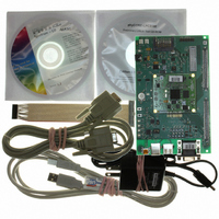
KIT DEV LPC3180
Manufacturer
NXP Semiconductors
Series
phyCORE®r
Type
MCUr
Datasheet
1.OM10096.pdf
(2 pages)
Specifications of OM10096
Contents
SBC Module, Carrier Board, Serial Cable, USB Cable, AC Adapter, and PHYTEC Spectrum CD
Lead Free Status / RoHS Status
Not applicable / Not applicable
For Use With/related Products
LPC3180
Lead Free Status / RoHS Status
Not applicable / Not applicable
Other names
568-4063
Available stocks
Company
Part Number
Manufacturer
Quantity
Price
Company:

Part Number:
OM10096Ј¬598
Manufacturer:
NXP
Quantity:
4


www.nxp.com
The on-chip memory management unit (MMU) supports major
operating systems, including Linux, the leading OS for embed-
ded applications. Also, the on-chip Java byte-code coproces-
sor supports basic security and authentication applications.
The vector floating-point coprocessor increases the speed of
typical calculations by a factor of four to five in scalar mode,
and much more in optimized vector mode.
Flexible power management enables high peak performance,
especially for floating-point calculations, and can be used to
shut down the core power domain while retaining real-time-
clock and wake-up functionality.
Multiple serial communications interfaces increase design flex-
ibility, provide larger buffer size, and deliver higher processing
power. The USB 2.0 device supports On-The-Go (OTG) and
has full speed host capabilities. There are seven 16C550 UARTs
(one supports IrDA), two Fast I
two SPI interfaces, and an automatic keyscan function that sup-
ports 8 x 8 keys.
There is a 10-bit A/D converter with three channels, two 32-bit
timers with four capture/compare channels, two PWM chan-
nels, a PLL, a real-time clock with separate clock and power
domain, a Watchdog timer, and a Secure Digital (SD) memory-
card interface. The core voltage supports 1.2 V, while the I/O
ports support 1.8 and 3.0 V. The operating temperature range
is -40 to 85 °C.
For debugging, the LPC3180 supports real-time emulation,
has an on-chip embedded-trace buffer with a 2K x 24-bit RAM,
and an integrated interrupt controller. Also, for compatibility
with existing tools, it uses the standard ARM test/debug JTAG
interface.
(1)
LPC3180 selection guide
Type
LPC3180
UART6 supports IrDA
External memory
interface
1
© 2006 NXP N.V.
All rights reserved. Reproduction in whole or in part is prohibited without the prior written consent of the copyright owner. The
information presented in this document does not form part of any quotation or contract, is believed to be accurate and reliable and
may be changed without notice. No liability will be accepted by the publisher for any consequence of its use. Publication thereof
does not convey nor imply any license under patent- or other industrial or intellectual property rights.
SRAM
2
64 KB
C-bus (400 Mbps) interfaces,
I-cache
32 K
D-cache
32 K
USB 2.0
(12 or 480 Mbps) + OTG
Third-Party Development Tools
Through third-party suppliers, we offer a range of develop-
ment tools for our microcontrollers. For the most current list-
ing, please visit www.nxp.com/microcontrollers.
LPC3180 block diagram
1
(NAND, SD, and DRAM)
(UART6 supports IrDA)
External Memory I/F
10-bit A/D Converter
Capture / Compare
(Three Channels)
Two timers with
32-K D Cache
(Master Only)
64-KB SRAM
UART 1-7
2 x I
Power Management, Real-time Clock,
DMA
2
Vector Floating–Point Coprocessor
C
I
2
2
C
Watchdog Timer, PLL
32-bit ARM926EJ-S
SPI
I/O ports (55)
2
Bus Matrix
UARTs
6
(1)
Date of release: October 2006
Document order number: 9397 750 15694
Printed in the USA
Embedded Trace Buffer
Full-speed / Host / OTG
E-ICE/RTM Interface
Interrupt Controller
ADC channels
(10-bit)
(1 Channel Each)
(Master Only)
32-K I Cache
USB 2.0
2 x PWM
Keyscan
2 x SPI
3
MMU
Package
LFBGA320
Related parts for OM10096
Image
Part Number
Description
Manufacturer
Datasheet
Request
R

Part Number:
Description:
NXP Semiconductors designed the LPC2420/2460 microcontroller around a 16-bit/32-bitARM7TDMI-S CPU core with real-time debug interfaces that include both JTAG andembedded trace
Manufacturer:
NXP Semiconductors
Datasheet:

Part Number:
Description:
NXP Semiconductors designed the LPC2458 microcontroller around a 16-bit/32-bitARM7TDMI-S CPU core with real-time debug interfaces that include both JTAG andembedded trace
Manufacturer:
NXP Semiconductors
Datasheet:
Part Number:
Description:
NXP Semiconductors designed the LPC2468 microcontroller around a 16-bit/32-bitARM7TDMI-S CPU core with real-time debug interfaces that include both JTAG andembedded trace
Manufacturer:
NXP Semiconductors
Datasheet:
Part Number:
Description:
NXP Semiconductors designed the LPC2470 microcontroller, powered by theARM7TDMI-S core, to be a highly integrated microcontroller for a wide range ofapplications that require advanced communications and high quality graphic displays
Manufacturer:
NXP Semiconductors
Datasheet:
Part Number:
Description:
NXP Semiconductors designed the LPC2478 microcontroller, powered by theARM7TDMI-S core, to be a highly integrated microcontroller for a wide range ofapplications that require advanced communications and high quality graphic displays
Manufacturer:
NXP Semiconductors
Datasheet:
Part Number:
Description:
The Philips Semiconductors XA (eXtended Architecture) family of 16-bit single-chip microcontrollers is powerful enough to easily handle the requirements of high performance embedded applications, yet inexpensive enough to compete in the market for hi
Manufacturer:
NXP Semiconductors
Datasheet:
Part Number:
Description:
The XA-S3 device is a member of Philips Semiconductors? XA(eXtended Architecture) family of high performance 16-bitsingle-chip microcontrollers
Manufacturer:
NXP Semiconductors
Datasheet:

Part Number:
Description:
The NXP BlueStreak LH75401/LH75411 family consists of two low-cost 16/32-bit System-on-Chip (SoC) devices
Manufacturer:
NXP Semiconductors
Datasheet:
Part Number:
Description:
The NXP LPC3130/3131 combine an 180 MHz ARM926EJ-S CPU core, high-speed USB2
Manufacturer:
NXP Semiconductors
Datasheet:
Part Number:
Description:
The NXP LPC3141 combine a 270 MHz ARM926EJ-S CPU core, High-speed USB 2
Manufacturer:
NXP Semiconductors
Part Number:
Description:
The NXP LPC3143 combine a 270 MHz ARM926EJ-S CPU core, High-speed USB 2
Manufacturer:
NXP Semiconductors

Part Number:
Description:
The NXP LPC3152 combines an 180 MHz ARM926EJ-S CPU core, High-speed USB 2
Manufacturer:
NXP Semiconductors
Part Number:
Description:
The NXP LPC3154 combines an 180 MHz ARM926EJ-S CPU core, High-speed USB 2
Manufacturer:
NXP Semiconductors

Part Number:
Description:
Standard level N-channel enhancement mode Field-Effect Transistor (FET) in a plastic package using NXP High-Performance Automotive (HPA) TrenchMOS technology
Manufacturer:
NXP Semiconductors
Datasheet: