TOOLSTICK560DC Silicon Laboratories Inc, TOOLSTICK560DC Datasheet - Page 210
TOOLSTICK560DC
Manufacturer Part Number
TOOLSTICK560DC
Description
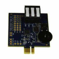
DAUGHTER CARD TOOLSTICK F560
Manufacturer
Silicon Laboratories Inc
Series
ToolStickr
Type
MCUr
Specifications of TOOLSTICK560DC
Contents
Daughter Card
Processor To Be Evaluated
C8051F55x, C8051F56x, C8051F57x
Interface Type
USB
Operating Supply Voltage
2.7 V to 3.6 V
Lead Free Status / RoHS Status
Lead free / RoHS Compliant
For Use With/related Products
C8051F55x, C8051F56x, C8051F57x
For Use With
336-1345 - TOOLSTICK BASE ADAPTER336-1182 - ADAPTER USB DEBUG FOR C8051FXXX
Lead Free Status / Rohs Status
Lead free / RoHS Compliant
Other names
336-1719


C8051F55x/56x/57x
The CAN controller clock must be less than or equal to 25 MHz. If the CIP-51 system clock is above
25 MHz, the divider in the CAN0CFG register must be set to divide the CAN controller clock down to an
appropriate speed.
21.1.2. CAN Register Access
The CAN controller clock divider selected in the CAN0CFG SFR affects how the CAN registers can be
accessed. If the divider is set to 1, then a CAN SFR can immediately be read after it is written. If the divider
is set to a value other than 1, then a read of a CAN SFR that has just been written must be delayed by a
certain number of cycles. This delay can be performed using a NOP or some other instruction that does
not attempt to read the register. This access limitation applies to read and read-modify-write instructions
that occur immediately after a write. The full list of affected instructions is ANL, ORL, MOV, XCH, and XRL.
For example, with the CAN0CFG divider set to 1, the CAN0CN SFR can be accessed as follows:
MOV CAN0CN, #041
MOV R7, CAN0CN
With the CAN0CFG divider set to /2, the same example code requires an additional NOP:
MOV CAN0CN, #041
NOP
MOV R7, CAN0CN
The number of delay cycles required is dependent on the divider setting. With a divider of 2, the read must
wait for 1 system clock cycle. With a divider of 4, the read must wait 3 system clock cycles, and with the
divider set to 8, the read must wait 7 system clock cycles. The delay only needs to be applied when read-
ing the same register that was written. The application can write and read other CAN SFRs without any
delay.
21.1.3. Example Timing Calculation for 1 Mbit/Sec Communication
This example shows how to configure the CAN controller timing parameters for a 1 Mbit/Sec bit rate.
Table 21.1 shows timing-related system parameters needed for the calculation.
Each bit transmitted on a CAN network has 4 segments (Sync_Seg, Prop_Seg, Phase_Seg1, and
Phase_Seg2), as shown in Figure 18.3. The sum of these segments determines the CAN bit time (1/bit
rate). In this example, the desired bit rate is 1 Mbit/sec; therefore, the desired bit time is 1000 ns.
210
CIP-51 system clock (SYSCLK)
CAN controller clock (f
CAN clock period (t
CAN time quantum (t
CAN bus length
Propogation delay time
Notes:
1. The CAN time quantum is the smallest unit of time recognized by the CAN controller. Bit timing parameters
2. The Baud Rate Prescaler (BRP) is defined as the value of the BRP Extension Register plus 1. The BRP
3. Based on an ISO-11898 compliant transceiver. CAN does not specify a physical layer.
are specified in integer multiples of the time quantum.
extension register has a reset value of 0x0000. The BRP has a reset value of 1.
Parameter
sys
q
)
)
sys
3
)
Table 21.1. Background System Information
; Enable access to Bit Timing Register
; Copy CAN0CN to R7
; Enable access to Bit Timing Register
; Wait for write to complete
; Copy CAN0CN to R7
41.667 ns
41.667 ns
24 MHz
24 MHz
400 ns
Value
10 m
Rev. 1.1
Internal Oscillator Max
CAN0CFG divider set to 1
Derived from 1/f
Derived from t
5 ns/m signal delay between CAN nodes
2 x (transceiver loop delay + bus line delay)
sys
sys
x BRP
Description
1,2
Related parts for TOOLSTICK560DC
Image
Part Number
Description
Manufacturer
Datasheet
Request
R

Part Number:
Description:
KIT TOOL EVAL SYS IN A USB STICK
Manufacturer:
Silicon Laboratories Inc
Datasheet:

Part Number:
Description:
TOOLSTICK DEBUG ADAPTER
Manufacturer:
Silicon Laboratories Inc
Datasheet:

Part Number:
Description:
TOOLSTICK BASE ADAPTER
Manufacturer:
Silicon Laboratories Inc
Datasheet:

Part Number:
Description:
TOOLSTICK DAUGHTER CARD
Manufacturer:
Silicon Laboratories Inc
Datasheet:

Part Number:
Description:
TOOLSTICK DAUGHTER CARD
Manufacturer:
Silicon Laboratories Inc
Datasheet:

Part Number:
Description:
TOOLSTICK DAUGHTER CARD
Manufacturer:
Silicon Laboratories Inc
Datasheet:

Part Number:
Description:
TOOLSTICK PROGRAMMING ADAPTER
Manufacturer:
Silicon Laboratories Inc
Datasheet:

Part Number:
Description:
TOOLSTICK DAUGHTER CARD
Manufacturer:
Silicon Laboratories Inc
Datasheet:

Part Number:
Description:
KIT STARTER TOOLSTICK
Manufacturer:
Silicon Laboratories Inc
Datasheet:

Part Number:
Description:
KIT UNIVERSITY TOOLSTICK STARTER
Manufacturer:
Silicon Laboratories Inc
Datasheet:

Part Number:
Description:
DAUGHTER CARD TOOLSTICK F330
Manufacturer:
Silicon Laboratories Inc
Datasheet:

Part Number:
Description:
CARD DAUGHTER UNIVRSTY TOOLSTICK
Manufacturer:
Silicon Laboratories Inc
Datasheet:

Part Number:
Description:
DAUGHTER CARD TOOLSTICK F582
Manufacturer:
Silicon Laboratories Inc
Datasheet:

Part Number:
Description:
DAUGHTER CARD TOOLSTICK F500
Manufacturer:
Silicon Laboratories Inc
Datasheet:

Part Number:
Description:
DAUGHTER CARD TOOLSTICK F540
Manufacturer:
Silicon Laboratories Inc
Datasheet: