TOOLSTICK560DC Silicon Laboratories Inc, TOOLSTICK560DC Datasheet - Page 6
TOOLSTICK560DC
Manufacturer Part Number
TOOLSTICK560DC
Description
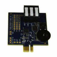
DAUGHTER CARD TOOLSTICK F560
Manufacturer
Silicon Laboratories Inc
Series
ToolStickr
Type
MCUr
Specifications of TOOLSTICK560DC
Contents
Daughter Card
Processor To Be Evaluated
C8051F55x, C8051F56x, C8051F57x
Interface Type
USB
Operating Supply Voltage
2.7 V to 3.6 V
Lead Free Status / RoHS Status
Lead free / RoHS Compliant
For Use With/related Products
C8051F55x, C8051F56x, C8051F57x
For Use With
336-1345 - TOOLSTICK BASE ADAPTER336-1182 - ADAPTER USB DEBUG FOR C8051FXXX
Lead Free Status / Rohs Status
Lead free / RoHS Compliant
Other names
336-1719


C8051F55x/56x/57x
22. SMBus................................................................................................................... 216
23. UART0 ................................................................................................................... 233
24. Enhanced Serial Peripheral Interface (SPI0) ..................................................... 242
25. Timers ................................................................................................................... 255
6
22.1. Supporting Documents .................................................................................. 217
22.2. SMBus Configuration..................................................................................... 217
22.3. SMBus Operation .......................................................................................... 217
22.4. Using the SMBus........................................................................................... 219
22.5. SMBus Transfer Modes................................................................................. 226
22.6. SMBus Status Decoding................................................................................ 230
23.1. Baud Rate Generator .................................................................................... 233
23.2. Data Format................................................................................................... 235
23.3. Configuration and Operation ......................................................................... 236
24.1. Signal Descriptions........................................................................................ 243
24.2. SPI0 Master Mode Operation ........................................................................ 244
24.3. SPI0 Slave Mode Operation .......................................................................... 246
24.4. SPI0 Interrupt Sources .................................................................................. 246
24.5. Serial Clock Phase and Polarity .................................................................... 247
24.6. SPI Special Function Registers ..................................................................... 248
25.1. Timer 0 and Timer 1 ...................................................................................... 257
21.2.2. Message Object Interface Registers ..................................................... 212
21.2.3. Message Handler Registers.................................................................. 212
21.2.4. CAN Register Assignment .................................................................... 213
22.3.1. Transmitter Vs. Receiver....................................................................... 218
22.3.2. Arbitration.............................................................................................. 218
22.3.3. Clock Low Extension............................................................................. 218
22.3.4. SCL Low Timeout.................................................................................. 218
22.3.5. SCL High (SMBus Free) Timeout ......................................................... 219
22.4.1. SMBus Configuration Register.............................................................. 219
22.4.2. SMB0CN Control Register .................................................................... 223
22.4.3. Data Register ........................................................................................ 226
22.5.1. Write Sequence (Master) ...................................................................... 227
22.5.2. Read Sequence (Master) ...................................................................... 228
22.5.3. Write Sequence (Slave) ........................................................................ 229
22.5.4. Read Sequence (Slave) ........................................................................ 230
23.3.1. Data Transmission ................................................................................ 236
23.3.2. Data Reception ..................................................................................... 236
23.3.3. Multiprocessor Communications ........................................................... 237
24.1.1. Master Out, Slave In (MOSI)................................................................. 243
24.1.2. Master In, Slave Out (MISO)................................................................. 243
24.1.3. Serial Clock (SCK) ................................................................................ 243
24.1.4. Slave Select (NSS) ............................................................................... 243
25.1.1. Mode 0: 13-bit Counter/Timer ............................................................... 257
25.1.2. Mode 1: 16-bit Counter/Timer ............................................................... 258
25.1.3. Mode 2: 8-bit Counter/Timer with Auto-Reload..................................... 258
Rev. 1.1
Related parts for TOOLSTICK560DC
Image
Part Number
Description
Manufacturer
Datasheet
Request
R

Part Number:
Description:
KIT TOOL EVAL SYS IN A USB STICK
Manufacturer:
Silicon Laboratories Inc
Datasheet:

Part Number:
Description:
TOOLSTICK DEBUG ADAPTER
Manufacturer:
Silicon Laboratories Inc
Datasheet:

Part Number:
Description:
TOOLSTICK BASE ADAPTER
Manufacturer:
Silicon Laboratories Inc
Datasheet:

Part Number:
Description:
TOOLSTICK DAUGHTER CARD
Manufacturer:
Silicon Laboratories Inc
Datasheet:

Part Number:
Description:
TOOLSTICK DAUGHTER CARD
Manufacturer:
Silicon Laboratories Inc
Datasheet:

Part Number:
Description:
TOOLSTICK DAUGHTER CARD
Manufacturer:
Silicon Laboratories Inc
Datasheet:

Part Number:
Description:
TOOLSTICK PROGRAMMING ADAPTER
Manufacturer:
Silicon Laboratories Inc
Datasheet:

Part Number:
Description:
TOOLSTICK DAUGHTER CARD
Manufacturer:
Silicon Laboratories Inc
Datasheet:

Part Number:
Description:
KIT STARTER TOOLSTICK
Manufacturer:
Silicon Laboratories Inc
Datasheet:

Part Number:
Description:
KIT UNIVERSITY TOOLSTICK STARTER
Manufacturer:
Silicon Laboratories Inc
Datasheet:

Part Number:
Description:
DAUGHTER CARD TOOLSTICK F330
Manufacturer:
Silicon Laboratories Inc
Datasheet:

Part Number:
Description:
CARD DAUGHTER UNIVRSTY TOOLSTICK
Manufacturer:
Silicon Laboratories Inc
Datasheet:

Part Number:
Description:
DAUGHTER CARD TOOLSTICK F582
Manufacturer:
Silicon Laboratories Inc
Datasheet:

Part Number:
Description:
DAUGHTER CARD TOOLSTICK F500
Manufacturer:
Silicon Laboratories Inc
Datasheet:

Part Number:
Description:
DAUGHTER CARD TOOLSTICK F540
Manufacturer:
Silicon Laboratories Inc
Datasheet: