C8051F040DK Silicon Laboratories Inc, C8051F040DK Datasheet - Page 4
C8051F040DK
Manufacturer Part Number
C8051F040DK
Description
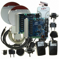
DEV KIT FOR F040/F041/F042/F043
Manufacturer
Silicon Laboratories Inc
Type
MCUr
Specifications of C8051F040DK
Contents
Evaluation Board, Power Supply, USB Cables, Adapter and Documentation
Processor To Be Evaluated
C8051F04x
Interface Type
USB
Silicon Manufacturer
Silicon Labs
Core Architecture
8051
Silicon Core Number
C8051F040
Silicon Family Name
C8051F04x
Lead Free Status / RoHS Status
Contains lead / RoHS non-compliant
For Use With/related Products
Silicon Laboratories C8051 F040, 041, 042, 043 MCUs
Lead Free Status / Rohs Status
Lead free / RoHS Compliant
Other names
336-1205
Available stocks
Company
Part Number
Manufacturer
Quantity
Price
Company:

Part Number:
C8051F040DK
Manufacturer:
SiliconL
Quantity:
9


C8051F040/1/2/3/4/5/6/7
8. DACs, 12-Bit Voltage Mode (C8051F040/1/2/3 Only) ......................................... 105
9. Voltage Reference (C8051F040/2/4/6) ................................................................. 113
10. Voltage Reference (C8051F041/3/5/7) ................................................................. 117
11. Comparators ......................................................................................................... 121
12. CIP-51 Microcontroller ......................................................................................... 127
13. Reset Sources....................................................................................................... 165
14. Oscillators ............................................................................................................. 173
4
8.1. DAC Output Scheduling.................................................................................. 106
8.2. DAC Output Scaling/Justification .................................................................... 106
11.1.Comparator Inputs.......................................................................................... 123
12.1.Instruction Set................................................................................................. 129
12.2.Memory Organization ..................................................................................... 133
12.3.Interrupt Handler............................................................................................. 153
12.4.Power Management Modes............................................................................ 163
13.1.Power-On Reset ............................................................................................. 166
13.2.Power-Fail Reset ............................................................................................ 166
13.3.External Reset ................................................................................................ 166
13.4.Missing Clock Detector Reset ........................................................................ 167
13.5.Comparator0 Reset ........................................................................................ 167
13.6.External CNVSTR0 Pin Reset ........................................................................ 167
13.7.Watchdog Timer Reset................................................................................... 167
14.1.Programmable Internal Oscillator ................................................................... 173
7.3.2. Window Detector in Differential Mode .................................................... 102
8.1.1. Update Output On-Demand ................................................................... 106
8.1.2. Update Output Based on Timer Overflow .............................................. 106
12.1.1.Instruction and CPU Timing ................................................................... 129
12.1.2.MOVX Instruction and Program Memory ............................................... 129
12.2.1.Program Memory ................................................................................... 133
12.2.2.Data Memory.......................................................................................... 134
12.2.3.General Purpose Registers.................................................................... 134
12.2.4.Bit Addressable Locations...................................................................... 134
12.2.5.Stack ..................................................................................................... 134
12.2.6.Special Function Registers .................................................................... 135
12.2.7.Register Descriptions ............................................................................. 150
12.3.1.MCU Interrupt Sources and Vectors ...................................................... 153
12.3.2.External Interrupts.................................................................................. 154
12.3.3.Interrupt Priorities................................................................................... 156
12.3.4.Interrupt Latency .................................................................................... 156
12.3.5.Interrupt Register Descriptions............................................................... 156
12.4.1.Idle Mode ............................................................................................... 163
12.4.2.Stop Mode.............................................................................................. 164
13.7.1.Enable/Reset WDT ................................................................................ 168
13.7.2.Disable WDT .......................................................................................... 168
13.7.3.Disable WDT Lockout ............................................................................ 168
13.7.4.Setting WDT Interval .............................................................................. 168
Rev. 1.5
Related parts for C8051F040DK
Image
Part Number
Description
Manufacturer
Datasheet
Request
R

Part Number:
Description:
SMD/C°/SINGLE-ENDED OUTPUT SILICON OSCILLATOR
Manufacturer:
Silicon Laboratories Inc
Part Number:
Description:
Manufacturer:
Silicon Laboratories Inc
Datasheet:
Part Number:
Description:
N/A N/A/SI4010 AES KEYFOB DEMO WITH LCD RX
Manufacturer:
Silicon Laboratories Inc
Datasheet:
Part Number:
Description:
N/A N/A/SI4010 SIMPLIFIED KEY FOB DEMO WITH LED RX
Manufacturer:
Silicon Laboratories Inc
Datasheet:
Part Number:
Description:
N/A/-40 TO 85 OC/EZLINK MODULE; F930/4432 HIGH BAND (REV E/B1)
Manufacturer:
Silicon Laboratories Inc
Part Number:
Description:
EZLink Module; F930/4432 Low Band (rev e/B1)
Manufacturer:
Silicon Laboratories Inc
Part Number:
Description:
I°/4460 10 DBM RADIO TEST CARD 434 MHZ
Manufacturer:
Silicon Laboratories Inc
Part Number:
Description:
I°/4461 14 DBM RADIO TEST CARD 868 MHZ
Manufacturer:
Silicon Laboratories Inc
Part Number:
Description:
I°/4463 20 DBM RFSWITCH RADIO TEST CARD 460 MHZ
Manufacturer:
Silicon Laboratories Inc
Part Number:
Description:
I°/4463 20 DBM RADIO TEST CARD 868 MHZ
Manufacturer:
Silicon Laboratories Inc
Part Number:
Description:
I°/4463 27 DBM RADIO TEST CARD 868 MHZ
Manufacturer:
Silicon Laboratories Inc
Part Number:
Description:
I°/4463 SKYWORKS 30 DBM RADIO TEST CARD 915 MHZ
Manufacturer:
Silicon Laboratories Inc
Part Number:
Description:
N/A N/A/-40 TO 85 OC/4463 RFMD 30 DBM RADIO TEST CARD 915 MHZ
Manufacturer:
Silicon Laboratories Inc
Part Number:
Description:
I°/4463 20 DBM RADIO TEST CARD 169 MHZ
Manufacturer:
Silicon Laboratories Inc