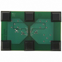
ADUM1100EVAL Analog Devices Inc, ADUM1100EVAL Datasheet - Page 10

ADUM1100EVAL
Manufacturer Part Number
ADUM1100EVAL
Description
BOARD EVAL FOR ADUM1100
Manufacturer
Analog Devices Inc
Type
Digital Isolatorr
Datasheet
1.ADUM1100ARZ-RL7.pdf
(20 pages)
Specifications of ADUM1100EVAL
Design Resources
USB Cable Isolator Circuit (CN0159)
Contents
Evaluation Board
For Use With/related Products
ADUM1100
Lead Free Status / RoHS Status
Contains lead / RoHS non-compliant
ADuM1100
DIN V VDE V 0884-10 (VDE V 0884-10):2006-12 INSULATION CHARACTERISTICS
This isolator is suitable for reinforced isolation, only within the safety limit data. Maintenance of the safety data is ensured by means of
protective circuits. The * marking on the package denotes DIN V VDE V 0884-10 approval for 560 V peak working voltage.
Table 7.
Description
Installation Classification per DIN VDE 0110
Climatic Classification
Pollution Degree per DIN VDE 0110, Table 1
Maximum Working Insulation Voltage
Input-to-Output Test Voltage, Method B1
Input-to-Output Test Voltage, Method A
Highest Allowable Overvoltage
Safety-Limiting Values
Insulation Resistance at T
Figure 2. Thermal Derating Curve, Dependence of Safety-Limiting Value
For Rated Mains Voltage ≤ 150 V rms
For Rated Mains Voltage ≤ 300 V rms
For Rated Mains Voltage ≤ 400 V rms
After Environmental Tests Subgroup 1
After Input and/or Safety Test Subgroup 2 and Subgroup 3
Case Temperature
Side 1 Current
Side 2 Current
180
160
140
120
100
80
60
40
20
0
0
with Case Temperature per DIN V VDE V 0884-10
INPUT CURRENT
50
S
OUTPUT CURRENT
CASE TEMPERATURE (°C)
100
150
200
Conditions
V
t
V
discharge < 5 pC
V
discharge < 5 pC
Transient overvoltage, t
Maximum value allowed in the event of a
failure (see
V
m
IORM
IORM
IORM
IO
= 1 sec, partial discharge < 5 pC
Rev. H | Page 10 of 20
= 500 V
× 1.875 = V
× 1.6 = V
× 1.2 = V
Figure 2
PR
PR
, t
, t
PR
RECOMMENDED OPERATING CONDITIONS
Table 8.
Parameter
Operating Temperature
Supply Voltages
Logic High Input Voltage,
Logic Low Input Voltage,
Logic High Input Voltage,
Logic Low Input Voltage,
Input Signal Rise and Fall Times
1
2
m
m
, 100% production test,
All voltages are relative to their respective ground.
Input switching thresholds have 300 mV of hysteresis. See the
Operation, DC Correctness, and Magnetic Field Immunity
and Figure 20 for information on immunity to external magnetic fields.
= 60 sec, partial
= 60 sec, partial
)
ADuM1100AR/ADuM1100BR
ADuM1100UR
5 V Operation
(See Figure 11 and Figure 12)
5 V Operation
(See Figure 11 and Figure 12)
3.3 V Operation
(See Figure 11 and Figure 12)
3.3 V Operation
(See Figure 11 and Figure 12)
TR
= 10 seconds
1
1, 2
1, 2
1, 2
1, 2
Symbol
V
V
V
V
T
I
I
R
S1
S2
S
IORM
PR
PR
TR
S
Symbol
T
T
V
V
V
V
V
V
A
A
DD1
DD2
IH
IL
IH
IL
,
Characteristic
I to IV
I to III
I to II
40/105/21
2
560
1050
896
672
4000
150
160
170
>10
9
Min
−40
−40
3.0
2.0
0.0
1.5
0.0
section,
Max
+105
+125
5.5
V
0.8
V
0.5
1.0
Method of
DD1
DD1
Figure 19
Unit
V peak
V peak
V peak
V peak
V peak
°C
mA
mA
Ω
Unit
°C
°C
V
V
V
V
V
ms
,


