ADUM1100EVAL Analog Devices Inc, ADUM1100EVAL Datasheet - Page 15
ADUM1100EVAL
Manufacturer Part Number
ADUM1100EVAL
Description
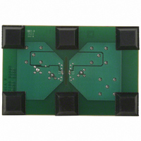
BOARD EVAL FOR ADUM1100
Manufacturer
Analog Devices Inc
Type
Digital Isolatorr
Datasheet
1.ADUM1100ARZ-RL7.pdf
(20 pages)
Specifications of ADUM1100EVAL
Design Resources
USB Cable Isolator Circuit (CN0159)
Contents
Evaluation Board
For Use With/related Products
ADUM1100
Lead Free Status / RoHS Status
Contains lead / RoHS non-compliant


APPLICATION INFORMATION
PC BOARD LAYOUT
The ADuM1100 digital isolator requires no external interface
circuitry for the logic interfaces. A bypass capacitor is recom-
mended at the input and output supply pins. The input bypass
capacitor can conveniently be connected between Pin 3 and
Pin 4 (see Figure 13). Alternatively, the bypass capacitor can be
located between Pin 1 and Pin 4. The output bypass capacitor
can be connected between Pin 7 and Pin 8 or Pin 5 and Pin 8.
The capacitor value should be between 0.01 μF and 0.1 μF. The
total lead length between both ends of the capacitor and the
power supply pins should not exceed 20 mm.
PROPAGATION DELAY-RELATED PARAMETERS
Propagation delay time describes the length of time it takes for
a logic signal to propagate through a component. Propagation
delay time to logic low output and propagation delay time to
logic high output refer to the duration between an input
signal transition and the respective output signal transition
(see Figure 14).
OUTPUT (V
INPUT (V
V
1
(DATA)
GND
V
DD1
O
I
Figure 13. Recommended Printed Circuit Board Layout
)
)
1
INPUT (V
Figure 14. Propagation Delay Parameters
I
V
)
ITH(L–H)
t
PLH
OUTPUT (V
V
I
∆
t
PHL
LH
O
)
(OPTIONAL)
t
PLH
Figure 15. Impact of Input Rise/Fall Time on Propagation Delay
50%
V
V
GND
t'
DD2
O
PLH
(DATA OUT)
50%
2
50%
Rev. H | Page 15 of 20
Pulse width distortion is the maximum difference between
t
input signal’s timing is preserved in the component’s output
signal. Propagation delay skew is the difference between the
minimum and maximum propagation delay values among
multiple ADuM1100 components operated at the same
operating temperature and having the same output load.
Depending on the input signal rise/fall time, the measured
propagation delay based on the input 50% level can vary from
the true propagation delay of the component (as measured from
its input switching threshold). This is because the input threshold,
as is the case with commonly used optocouplers, is at a different
voltage level than the 50% point of typical input signals. This
propagation delay difference is given by
where:
t
input 50% level.
t’
input switching thresholds.
t
V
V
PLH
PLH
R
PLH
I
ITH (L–H
and t
is the amplitude of the input signal (0 to V
and t
and t
and t’
Δ
Δ
LH
HL
F
and, V
= t′
= t′
are the input 10% to 90% rise/fall times.
PHL
PHL
50%
PHL
∆
V
HL
ITH(H–L)
PLH
PHL
are the propagation delays as measured from the
and provides an indication of how accurately the
are the propagation delays as measured from the
ITH (H–L)
− t
− t
PLH
PHL
t
PHL
= (t
= (t
are the input switching thresholds.
R
F
/0.8 V
/0.8 V
t'
PHL
I
I
)(0.5 V
)(0.5 V
1
1
− V
− V
ITH (L-H)
ITH (H-L)
I
levels assumed).
ADuM1100
)
)
Related parts for ADUM1100EVAL
Image
Part Number
Description
Manufacturer
Datasheet
Request
R

Part Number:
Description:
±1.7g Dual-Axis IMEMS Accelerometer Evaluation Board
Manufacturer:
Analog Devices Inc
Datasheet:

Part Number:
Description:
Inertial Sensor Evaluation System
Manufacturer:
Analog Devices Inc
Datasheet:
Part Number:
Description:
Manufacturer:
Analog Devices Inc
Datasheet:
Part Number:
Description:
Manufacturer:
Analog Devices Inc
Datasheet:
Part Number:
Description:
Manufacturer:
Analog Devices Inc
Datasheet:
Part Number:
Description:
Manufacturer:
Analog Devices Inc
Datasheet:
Part Number:
Description:
Manufacturer:
Analog Devices Inc
Datasheet:
Part Number:
Description:
Manufacturer:
Analog Devices Inc
Datasheet:
Part Number:
Description:
Manufacturer:
Analog Devices Inc
Datasheet:
Part Number:
Description:
Manufacturer:
Analog Devices Inc
Datasheet:
Part Number:
Description:
Manufacturer:
Analog Devices Inc
Datasheet:
Part Number:
Description:
Manufacturer:
Analog Devices Inc
Datasheet:
Part Number:
Description:
Manufacturer:
Analog Devices Inc
Datasheet: