ADUM1100EVAL Analog Devices Inc, ADUM1100EVAL Datasheet - Page 3
ADUM1100EVAL
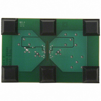
Manufacturer Part Number
ADUM1100EVAL
Description
BOARD EVAL FOR ADUM1100
Manufacturer
Analog Devices Inc
Type
Digital Isolatorr
Datasheet
1.ADUM1100ARZ-RL7.pdf
(20 pages)
Specifications of ADUM1100EVAL
Design Resources
USB Cable Isolator Circuit (CN0159)
Contents
Evaluation Board
For Use With/related Products
ADUM1100
Lead Free Status / RoHS Status
Contains lead / RoHS non-compliant


SPECIFICATIONS
ELECTRICAL SPECIFICATIONS—5 V OPERATION
All voltages are relative to their respective ground. 4.5 V ≤ V
apply over the entire recommended operation range, unless otherwise noted. All typical specifications are at T
Table 1.
Parameter
DC SPECIFICATIONS
SWITCHING SPECIFICATIONS
Input Supply Current
Output Supply Current
Input Supply Current (25 Mbps)
Output Supply Current
Input Supply Current (100 Mbps)
Output Supply Current
Input Current
Logic High Output Voltage
Logic Low Output Voltage
For ADuM1100AR
For ADuM1100BR/ADuM1100UR
For All Grades
(See Figure 5)
(See Figure 6)
(See Figure 5)
(See Figure 6)
Minimum Pulse Width
Maximum Data Rate
Minimum Pulse Width
Maximum Data Rate
Propagation Delay Time to Logic Low
Propagation Delay Time to Logic High
Pulse Width Distortion |t
Change vs. Temperature
Propagation Delay Skew
Propagation Delay Skew
Output Rise/Fall Time
Common-Mode Transient Immunity
Refresh Rate
Input Dynamic Supply Current
Output Dynamic Supply Current
Output
Output
(Equal Temperature)
(Equal Temperature, Supplies)
at Logic Low/High Output
4, 5
4, 5
(See Figure 7)
(See Figure 7)
1
3
1
3
(100 Mbps)
(25 Mbps)
2
2
5, 7
PLH
6
– t
8
PHL
9
|
5, 7
9
5
Symbol
I
I
I
I
I
I
I
V
V
PW
PW
t
t
PWD
t
t
t
|CM
|CM
f
I
I
DD1 (Q)
DD2 (Q)
DD1 (25)
DD2 (25)
DD1 (100)
DD2 (100)
I
DDI (D)
DDO (D)
r
PHL
PLH
PSK1
PSK2
R
OH
OL
, t
F
L
H
|,
|
Min
−10
V
V
25
100
25
DD2
DD2
DD1
Rev. H | Page 3 of 20
− 0.1
− 0.8
≤ 5.5 V, 4.5 V ≤ V
Typ
0.3
0.01
2.2
0.5
9.0
2.0
+0.01
5.0
4.6
0.0
0.03
0.3
6.7
150
10.5
10.5
0.5
3
3
35
1.2
0.09
0.02
Max
0.8
0.06
3.5
1.0
14
2.8
+10
0.1
0.1
0.8
40
10
18
18
2
8
6
DD2
≤ 5.5 V. All minimum/maximum specifications
Unit
mA
mA
mA
mA
mA
mA
μA
V
V
V
V
V
ns
Mbps
ns
Mbps
ns
ns
ns
ps/°C
ns
ns
ns
kV/μs
Mbps
mA/Mbps
mA/Mbps
Test Conditions
V
V
12.5 MHz logic signal frequency
12.5 MHz logic signal frequency
50 MHz logic signal frequency,
ADuM1100BR/ADuM1100UR only
50 MHz logic signal frequency,
ADuM1100BR/ADuM1100UR only
0 V ≤ V
I
I
I
I
I
C
C
C
C
C
C
C
C
C
C
C
V
transient magnitude = 800 V
O
O
O
O
O
I
I
L
L
L
L
L
L
L
L
L
L
L
I
= 0 V or V
= 0 V or V
= −20 μA, V
= −4 mA, V
= 20 μA, V
= 400 μA, V
= 4 mA, V
= 0 V or V
= 15 pF, CMOS signal levels
= 15 pF, CMOS signal levels
= 15 pF, CMOS signal levels
= 15 pF, CMOS signal levels
= 15 pF, CMOS signal levels
= 15 pF, CMOS signal levels
= 15 pF, CMOS signal levels
= 15 pF, CMOS signal levels
= 15 pF, CMOS signal levels
= 15 pF, CMOS signal levels
= 15 pF, CMOS signal levels
IN
≤ V
A
= 25°C, V
DD1
DD1
I
DD1
DD1
I
= V
I
= V
I
I
= V
= V
, V
= V
IL
IL
CM
IH
IL
IH
= 1000 V,
ADuM1100
DD1
= V
DD2
= 5 V.
Related parts for ADUM1100EVAL
Image
Part Number
Description
Manufacturer
Datasheet
Request
R

Part Number:
Description:
±1.7g Dual-Axis IMEMS Accelerometer Evaluation Board
Manufacturer:
Analog Devices Inc
Datasheet:

Part Number:
Description:
Inertial Sensor Evaluation System
Manufacturer:
Analog Devices Inc
Datasheet:
Part Number:
Description:
Manufacturer:
Analog Devices Inc
Datasheet:
Part Number:
Description:
Manufacturer:
Analog Devices Inc
Datasheet:
Part Number:
Description:
Manufacturer:
Analog Devices Inc
Datasheet:
Part Number:
Description:
Manufacturer:
Analog Devices Inc
Datasheet:
Part Number:
Description:
Manufacturer:
Analog Devices Inc
Datasheet:
Part Number:
Description:
Manufacturer:
Analog Devices Inc
Datasheet:
Part Number:
Description:
Manufacturer:
Analog Devices Inc
Datasheet:
Part Number:
Description:
Manufacturer:
Analog Devices Inc
Datasheet:
Part Number:
Description:
Manufacturer:
Analog Devices Inc
Datasheet:
Part Number:
Description:
Manufacturer:
Analog Devices Inc
Datasheet:
Part Number:
Description:
Manufacturer:
Analog Devices Inc
Datasheet: