EVAL-AD7654CB Analog Devices Inc, EVAL-AD7654CB Datasheet - Page 2
EVAL-AD7654CB
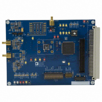
Manufacturer Part Number
EVAL-AD7654CB
Description
BOARD EVAL FOR AD7654
Manufacturer
Analog Devices Inc
Series
PulSAR®r
Specifications of EVAL-AD7654CB
Number Of Adc's
2
Number Of Bits
16
Sampling Rate (per Second)
500k
Data Interface
Serial, Parallel
Inputs Per Adc
2 Differential
Input Range
0 ~ 5 V
Power (typ) @ Conditions
120mW @ 500kSPS
Voltage Supply Source
Analog and Digital
Operating Temperature
-40°C ~ 85°C
Utilized Ic / Part
AD7654
Lead Free Status / RoHS Status
Contains lead / RoHS non-compliant


AD7654
TABLE OF CONTENTS
Features .............................................................................................. 1
Applications....................................................................................... 1
Functional Block Diagram .............................................................. 1
General Description ......................................................................... 1
Product Highlights ........................................................................... 1
Specifications..................................................................................... 3
Absolute Maximum Ratings............................................................ 7
Pin Configuration and Function Descriptions............................. 8
Terminology .................................................................................... 11
Typical Performance Characteristics ........................................... 12
Application Information................................................................ 14
REVISION HISTORY
11/05—Rev. A to Rev. B
Changes to General Description .................................................... 1
Changes to Timing Specifications .................................................. 5
Changes to Figure 16...................................................................... 13
Changes to Figure 18...................................................................... 15
Added Table 8.................................................................................. 17
Changes to Figure 24...................................................................... 19
Changes to Figure 29...................................................................... 21
Updated Outline Dimensions ....................................................... 26
Changes to Ordering Guide .......................................................... 26
Timing Specifications .................................................................. 5
ESD Caution.................................................................................. 7
Circuit Information.................................................................... 14
Modes of Operation ................................................................... 14
Transfer Functions...................................................................... 14
Typical Connection Diagram ................................................... 16
Analog Inputs.............................................................................. 16
Input Channel Multiplexer........................................................ 16
Rev. B | Page 2 of 28
Application Hints ........................................................................... 25
Outline Dimensions ....................................................................... 26
11/04—Rev. 0 to Rev. A
Changes to Figure 7........................................................................ 12
Changes to Figure 18...................................................................... 15
Changes to Figure 19...................................................................... 16
Changes to Voltage Reference Input Section .............................. 17
Changes to Conversion Control Section..................................... 18
Changes to Digital Interface Section ........................................... 18
Updated Outline Dimensions...................................................... 25
11/02—Revision 0: Initial Version
Driver Amplifier Choice ........................................................... 16
Voltage Reference Input ............................................................ 17
Power Supply............................................................................... 17
Power Dissipation....................................................................... 17
Conversion Control ................................................................... 18
Digital Interface.......................................................................... 18
Parallel Interface......................................................................... 18
Serial Interface ............................................................................ 20
Master Serial Interface............................................................... 20
Slave Serial Interface .................................................................. 22
Microprocessor Interfacing....................................................... 24
SPI Interface (ADSP-219x) ....................................................... 24
Layout .......................................................................................... 25
Evaluating the AD7654 Performance ...................................... 25
Ordering Guide .......................................................................... 27
Related parts for EVAL-AD7654CB
Image
Part Number
Description
Manufacturer
Datasheet
Request
R

Part Number:
Description:
ENERCHIP CC EVAL KIT
Manufacturer:
Cymbet Corporation
Datasheet:

Part Number:
Description:
BOARD EVAL FOR AD976
Manufacturer:
Analog Devices Inc
Datasheet:

Part Number:
Description:
BOARD EVAL FOR ADXL345
Manufacturer:
Analog Devices Inc
Datasheet:

Part Number:
Description:
ENERCHIP CC SEH EVAL KIT
Manufacturer:
Cymbet Corporation
Datasheet:

Part Number:
Description:
ENERCHIP EP ENERGY HARVEST EVAL
Manufacturer:
Cymbet Corporation
Datasheet:

Part Number:
Description:
EVAL BOARD FOR TW6864-LB2-GR
Manufacturer:
Intersil
Datasheet:
Part Number:
Description:
EVAL BOARD FOR TW8816-LB3-GR
Manufacturer:
Intersil
Datasheet:
Part Number:
Description:
EVAL BOARD FOR TW8817-TA3-GRS
Manufacturer:
Intersil
Datasheet:

Part Number:
Description:
EVALUATION MODULE FOR ADUM4160
Manufacturer:
Analog Devices Inc
Datasheet:

Part Number:
Description:
BOARD EVALUATION ADCMP581BCP
Manufacturer:
Analog Devices Inc
Datasheet:
Part Number:
Description:
BOARD EVALUATION ADM1041
Manufacturer:
Analog Devices Inc
Datasheet:

Part Number:
Description:
EVAL BOARD FOR STM32F107VCT
Manufacturer:
STMicroelectronics
Datasheet:
Part Number:
Description:
BOARD EVAL FOR AD1954
Manufacturer:
Analog Devices Inc
Datasheet:
Part Number:
Description:
BOARD EVAL FOR AD1955
Manufacturer:
Analog Devices Inc
Datasheet:

Part Number:
Description:
BOARD EVAL FOR AD7655
Manufacturer:
Analog Devices Inc
Datasheet: