EVAL-AD7654CB Analog Devices Inc, EVAL-AD7654CB Datasheet - Page 20
EVAL-AD7654CB
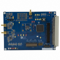
Manufacturer Part Number
EVAL-AD7654CB
Description
BOARD EVAL FOR AD7654
Manufacturer
Analog Devices Inc
Series
PulSAR®r
Specifications of EVAL-AD7654CB
Number Of Adc's
2
Number Of Bits
16
Sampling Rate (per Second)
500k
Data Interface
Serial, Parallel
Inputs Per Adc
2 Differential
Input Range
0 ~ 5 V
Power (typ) @ Conditions
120mW @ 500kSPS
Voltage Supply Source
Analog and Digital
Operating Temperature
-40°C ~ 85°C
Utilized Ic / Part
AD7654
Lead Free Status / RoHS Status
Contains lead / RoHS non-compliant


AD7654
SERIAL INTERFACE
The AD7654 is configured to use the serial interface when the
SER/ PAR is held high. The AD7654 outputs 32 bits of data,
MSB first, on the SDOUT pin. The order of the channels being
output is also controlled by A/ B . When high, Channel A is
output first; when low, Channel B is output first. This data
is synchronized with the 32 clock pulses provided on the
SCLK pin.
MASTER SERIAL INTERFACE
Internal Clock
The AD7654 is configured to generate and provide the serial
data clock SCLK when the EXT/ INT pin is held low. The
AD7654 also generates a SYNC signal to indicate to the host
when the serial data is valid. The serial clock SCLK and the
SYNC signal can be inverted if desired. The output data is valid
on both the rising and falling edge of the data clock. Depending
on RDC/SDIN input, the data can be read after each conversion
or during the following conversion. Figure 29 and Figure 30
show the detailed timing diagrams of these two modes.
Rev. B | Page 20 of 28
Usually, because the AD7654 is used with a fast throughput, the
master-read-during-convert mode is the most recommended
serial mode when it can be used. In this mode, the serial clock
and data toggle at appropriate instants, which minimizes
potential feedthrough between digital activity and the critical
conversion decisions. The SYNC signal goes low after the LSB
of each channel has been output. Note that in this mode, the
SCLK period changes because the LSBs require more time to
settle, and the SCLK is derived from the SAR conversion clock.
Note that in the master-read-after-convert mode, unlike in
other modes, the signal BUSY returns low after the 32 data bits
are pulsed out and not at the end of the conversion phase,
which results in a longer BUSY width. One advantage of using
this mode is that it can accommodate slow digital hosts because
the serial clock can be slowed down by using DIVSCLK[1:0]
inputs. Refer to Table 4 for the timing details.
Related parts for EVAL-AD7654CB
Image
Part Number
Description
Manufacturer
Datasheet
Request
R

Part Number:
Description:
ENERCHIP CC EVAL KIT
Manufacturer:
Cymbet Corporation
Datasheet:

Part Number:
Description:
BOARD EVAL FOR AD976
Manufacturer:
Analog Devices Inc
Datasheet:

Part Number:
Description:
BOARD EVAL FOR ADXL345
Manufacturer:
Analog Devices Inc
Datasheet:

Part Number:
Description:
ENERCHIP CC SEH EVAL KIT
Manufacturer:
Cymbet Corporation
Datasheet:

Part Number:
Description:
ENERCHIP EP ENERGY HARVEST EVAL
Manufacturer:
Cymbet Corporation
Datasheet:

Part Number:
Description:
EVAL BOARD FOR TW6864-LB2-GR
Manufacturer:
Intersil
Datasheet:
Part Number:
Description:
EVAL BOARD FOR TW8816-LB3-GR
Manufacturer:
Intersil
Datasheet:
Part Number:
Description:
EVAL BOARD FOR TW8817-TA3-GRS
Manufacturer:
Intersil
Datasheet:

Part Number:
Description:
EVALUATION MODULE FOR ADUM4160
Manufacturer:
Analog Devices Inc
Datasheet:

Part Number:
Description:
BOARD EVALUATION ADCMP581BCP
Manufacturer:
Analog Devices Inc
Datasheet:
Part Number:
Description:
BOARD EVALUATION ADM1041
Manufacturer:
Analog Devices Inc
Datasheet:

Part Number:
Description:
EVAL BOARD FOR STM32F107VCT
Manufacturer:
STMicroelectronics
Datasheet:
Part Number:
Description:
BOARD EVAL FOR AD1954
Manufacturer:
Analog Devices Inc
Datasheet:
Part Number:
Description:
BOARD EVAL FOR AD1955
Manufacturer:
Analog Devices Inc
Datasheet:

Part Number:
Description:
BOARD EVAL FOR AD7655
Manufacturer:
Analog Devices Inc
Datasheet: