MC56F8323EVM Freescale Semiconductor, MC56F8323EVM Datasheet - Page 22
MC56F8323EVM
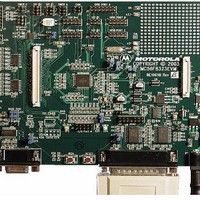
Manufacturer Part Number
MC56F8323EVM
Description
KIT EVALUATION FOR MC56F8323
Manufacturer
Freescale Semiconductor
Type
DSPr
Datasheets
1.CWH-UTP-ONCE-HE.pdf
(2 pages)
2.MC56F8323EVM.pdf
(72 pages)
3.MC56F8323EVME.pdf
(140 pages)
Specifications of MC56F8323EVM
Contents
Module and Misc Hardware
Processor To Be Evaluated
MC56F8322 and MC56F8323
Data Bus Width
16 bit
Interface Type
RS-232
For Use With/related Products
MC56F8322, MC56F8323
Lead Free Status / RoHS Status
Contains lead / RoHS non-compliant


22
Signal Name
(SYS_CLK2)
(SYS_CLK)
PHASEB0
(GPIOB6)
(GPIOB5)
INDEX0
(TA1)
(TA2)
Table 2-2 Signal and Package Information for the 64-Pin LQFP
Pin No.
51
50
Schmitt
Schmitt
Schmitt
Schmitt
Schmitt
Schmitt
Output
Output
Output
Output
Output
Output
Input/
Input/
Input/
Input/
Type
Input
Input
State During
enabled
enabled
pull-up
pull-up
Reset
56F8323 Technical Data, Rev. 17
Input,
Input,
Phase B — Quadrature Decoder 0, PHASEB input
TA1 — Timer A ,Channel 1
Port B GPIO — This GPIO pin can be individually programmed as
an input or output pin.
Clock Output - can be used to monitor the internal SYS_CLK2
signal (see
In the 56F8323, the default state after reset is PHASEB0.
In the 56F8123, the default state is not one of the functions offered
and must be reconfigured.
Index — Quadrature Decoder 0, INDEX input
TA2 — Timer A, Channel 2
Port B GPIO — This GPIO pin can be individually programmed as
an input or output pin.
Clock Output - can be used to monitor the internal SYS_CLK signal
(see
In the 56F8323, the default state after reset is INDEX0.
In the 56F8123, the default state is not one of the functions offered
and must be reconfigured.
Part 6.5.7
Part 6.5.7
CLKO Select Register, SIM_CLKOSR).
CLKO Select Register, SIM_CLKOSR).
Signal Description
Freescale Semiconductor
Preliminary
Related parts for MC56F8323EVM
Image
Part Number
Description
Manufacturer
Datasheet
Request
R

Part Number:
Description:
Manufacturer:
Freescale Semiconductor, Inc
Datasheet:
Part Number:
Description:
Manufacturer:
Freescale Semiconductor, Inc
Datasheet:
Part Number:
Description:
Manufacturer:
Freescale Semiconductor, Inc
Datasheet:
Part Number:
Description:
Manufacturer:
Freescale Semiconductor, Inc
Datasheet:
Part Number:
Description:
Manufacturer:
Freescale Semiconductor, Inc
Datasheet:
Part Number:
Description:
Manufacturer:
Freescale Semiconductor, Inc
Datasheet:
Part Number:
Description:
Manufacturer:
Freescale Semiconductor, Inc
Datasheet:
Part Number:
Description:
Manufacturer:
Freescale Semiconductor, Inc
Datasheet:
Part Number:
Description:
Manufacturer:
Freescale Semiconductor, Inc
Datasheet:
Part Number:
Description:
Manufacturer:
Freescale Semiconductor, Inc
Datasheet:
Part Number:
Description:
Manufacturer:
Freescale Semiconductor, Inc
Datasheet:
Part Number:
Description:
Manufacturer:
Freescale Semiconductor, Inc
Datasheet:
Part Number:
Description:
Manufacturer:
Freescale Semiconductor, Inc
Datasheet:
Part Number:
Description:
Manufacturer:
Freescale Semiconductor, Inc
Datasheet:
Part Number:
Description:
Manufacturer:
Freescale Semiconductor, Inc
Datasheet: