HW-SPAR3-SK-UNI-G Xilinx Inc, HW-SPAR3-SK-UNI-G Datasheet - Page 39
HW-SPAR3-SK-UNI-G
Manufacturer Part Number
HW-SPAR3-SK-UNI-G
Description
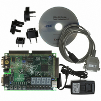
KIT STARTER SPARTAN-3
Manufacturer
Xilinx Inc
Series
Spartan-3r
Type
FPGA Configurationr
Datasheet
1.HW-SPAR3-SK-UNI-G.pdf
(64 pages)
Specifications of HW-SPAR3-SK-UNI-G
Contents
Board, Cable, Software, Datasheets and User Manual
For Use With/related Products
Spartan-3
Lead Free Status / RoHS Status
Lead free / RoHS Compliant
Other names
122-1521
Available stocks
Company
Part Number
Manufacturer
Quantity
Price


“Flash Read” Option
“Flash Read” Option
Spartan-3 FPGA Starter Kit Board User Guide
UG130 (v1.2) June 20, 2008
The Spartan-3 Starter Kit Board includes a 2Mbit Platform Flash configuration PROM. The
XC3S200 FPGA on the board only requires slightly less than 1Mbit for configuration data.
The remainder of the Platform Flash is available to store other non-volatile data, such as
revision codes, serial numbers, coefficients, an Ethernet MAC ID, or code for an embedded
processor, such as MicroBlaze, within the FPGA.
To allow the FPGA to read from Platform Flash after configuration, the JP1 jumper must be
properly positioned, as shown in
Platform Flash is always enabled. After FPGA configuration completes, the FPGA
application drives the INIT_B pin High, FPGA pin N9. Consequently, the Platform Flash
data pointer is not reset and points to the additional data following the FPGA
configuration data. To read any subsequent data, the FPGA application generates
additional clock pulses on the RCLK signal from FPGA pin A14. After configuration, the
FPGA’s CCLK output is three-stated with a pull-up resistor to V
Platform Flash presents serial data on the FPGA’s DIN pin, pin M11.
The resistor between the CCLK output and FPGA pin A14 prevents any accidental
conflicts between the two signals.
Figure 10-2: Read Additional Data from Platform Flash by Setting the JP1 Jumper
J8
J8
M0
M1
M2
M0
M1
M2
Spartan-3 FPGA
Spartan-3 FPGA
Figure 10-1: Default Platform Flash Option
www.xilinx.com
USER I/O
USER I/O
DIN/D0
DIN/D0
INIT_B
INIT_B
DONE
DONE
CCLK
CCLK
Figure
RCLK
RCLK
(xx) = FPGA pin number
10-2. When the jumper is in this position, the
(M11)
(N9)
(A14)
D0
OE/RESET
CE
CLK
D0
OE/RESET
CE
CLK
Platform Flash
Platform Flash
CCAUX
(2.5V). The
Flash Read
UG130_c10_02_060404
UG130_c10_01_060704
Default
JP1
JP1
39
R
Related parts for HW-SPAR3-SK-UNI-G
Image
Part Number
Description
Manufacturer
Datasheet
Request
R

Part Number:
Description:
STARTER KIT BUNDLE SPARTAN3/CPLD
Manufacturer:
Xilinx Inc
Part Number:
Description:
KIT HDWR FOR SPARTAN3/CPLD-JAPAN
Manufacturer:
Xilinx Inc

Part Number:
Description:
IC CPLD .8K 36MCELL 44-VQFP
Manufacturer:
Xilinx Inc
Datasheet:

Part Number:
Description:
IC CPLD 72MCRCELL 10NS 44VQFP
Manufacturer:
Xilinx Inc
Datasheet:

Part Number:
Description:
IC CPLD 1.6K 72MCELL 64-VQFP
Manufacturer:
Xilinx Inc
Datasheet:

Part Number:
Description:
IC CR-II CPLD 64MCELL 44-VQFP
Manufacturer:
Xilinx Inc
Datasheet:

Part Number:
Description:
IC CPLD 1.6K 72MCELL 100-TQFP
Manufacturer:
Xilinx Inc
Datasheet:

Part Number:
Description:
IC CR-II CPLD 64MCELL 56-BGA
Manufacturer:
Xilinx Inc
Datasheet:

Part Number:
Description:
IC CPLD 72MCRCELL 7.5NS 44VQFP
Manufacturer:
Xilinx Inc
Datasheet:
Part Number:
Description:
IC CR-II CPLD 64MCELL 100-VQFP
Manufacturer:
Xilinx Inc
Datasheet:
Part Number:
Description:
IC CPLD 1.6K 72MCELL 100-TQFP
Manufacturer:
Xilinx Inc
Datasheet:

Part Number:
Description:
IC CPLD 72MCRCELL 7.5NS 64VQFP
Manufacturer:
Xilinx Inc
Datasheet:
Part Number:
Description:
IC CPLD 1.6K 72MCELL 100-TQFP
Manufacturer:
Xilinx Inc
Datasheet:

Part Number:
Description:
IC CPLD 1.5K 64MCELL HP 44-VQFP
Manufacturer:
Xilinx Inc

Part Number:
Description:
IC CPLD 36MCRCELL 15NS 44PLCC
Manufacturer:
Xilinx Inc
Datasheet: