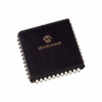
PIC18F442-I/L Microchip Technology, PIC18F442-I/L Datasheet - Page 109

PIC18F442-I/L
Manufacturer Part Number
PIC18F442-I/L
Description
IC MCU FLASH 8KX16 EE A/D 44PLCC
Manufacturer
Microchip Technology
Series
PIC® 18Fr
Datasheets
1.PIC16F616T-ISL.pdf
(8 pages)
2.PIC18F242-ISO.pdf
(332 pages)
3.PIC18F242-ISO.pdf
(14 pages)
4.PIC18F242-ISO.pdf
(16 pages)
5.PIC18F242-ISO.pdf
(16 pages)
6.PIC18F242-ISO.pdf
(14 pages)
7.PIC18LF242-ISO.pdf
(36 pages)
Specifications of PIC18F442-I/L
Core Size
8-Bit
Program Memory Size
16KB (8K x 16)
Core Processor
PIC
Speed
40MHz
Connectivity
I²C, SPI, UART/USART
Peripherals
Brown-out Detect/Reset, LVD, POR, PWM, WDT
Number Of I /o
34
Program Memory Type
FLASH
Eeprom Size
256 x 8
Ram Size
768 x 8
Voltage - Supply (vcc/vdd)
4.2 V ~ 5.5 V
Data Converters
A/D 8x10b
Oscillator Type
External
Operating Temperature
-40°C ~ 85°C
Package / Case
44-PLCC
Controller Family/series
PIC18
No. Of I/o's
34
Eeprom Memory Size
256Byte
Ram Memory Size
768Byte
Cpu Speed
40MHz
No. Of Timers
4
Processor Series
PIC18F
Core
PIC
Data Bus Width
8 bit
Data Ram Size
768 B
Interface Type
MSSP, SPI, I2C, PSP, USART
Maximum Clock Frequency
40 MHz
Number Of Programmable I/os
34
Number Of Timers
1 x 16 bit
Operating Supply Voltage
2 V to 5.5 V
Maximum Operating Temperature
+ 85 C
Mounting Style
SMD/SMT
3rd Party Development Tools
52715-96, 52716-328, 52717-734, 52712-325, EWPIC18
Development Tools By Supplier
PG164130, DV164035, DV244005, DV164005, PG164120, ICE2000, ICE4000, DM163022, DV164136
Minimum Operating Temperature
- 40 C
On-chip Adc
8
Package
44PLCC
Device Core
PIC
Family Name
PIC18
Maximum Speed
40 MHz
Lead Free Status / RoHS Status
Lead free / RoHS Compliant
For Use With
AC164309 - MODULE SKT FOR PM3 44PLCCXLT44L2 - SOCKET TRAN ICE 44PLCC444-1001 - DEMO BOARD FOR PICMICRO MCUDVA16XL441 - ADAPTER DEVICE ICE 44PLCCDV007003 - PROGRAMMER UNIVERSAL PROMATE II
Lead Free Status / Rohs Status
Details
Other names
PIC18F442I/L
Available stocks
Company
Part Number
Manufacturer
Quantity
Price
Company:
Part Number:
PIC18F442-I/L
Manufacturer:
Microchip Technology
Quantity:
10 000
- PIC16F616T-ISL PDF datasheet
- PIC18F242-ISO PDF datasheet #2
- PIC18F242-ISO PDF datasheet #3
- PIC18F242-ISO PDF datasheet #4
- PIC18F242-ISO PDF datasheet #5
- PIC18F242-ISO PDF datasheet #6
- PIC18LF242-ISO PDF datasheet #7
- Current page: 109 of 332
- Download datasheet (6Mb)
11.0
The Timer1 module timer/counter has the following
features:
• 16-bit timer/counter
• Readable and writable (both registers)
• Internal or external clock select
• Interrupt-on-overflow from FFFFh to 0000h
• RESET from CCP module special event trigger
REGISTER 11-1:
© 2006 Microchip Technology Inc.
(two 8-bit registers; TMR1H and TMR1L)
TIMER1 MODULE
bit 7
bit 6
bit 5-4
bit 3
bit 2
bit 1
bit 0
RD16: 16-bit Read/Write Mode Enable bit
1 = Enables register Read/Write of Timer1 in one 16-bit operation
0 = Enables register Read/Write of Timer1 in two 8-bit operations
Unimplemented: Read as '0'
T1CKPS1:T1CKPS0: Timer1 Input Clock Prescale Select bits
11 = 1:8 Prescale value
10 = 1:4 Prescale value
01 = 1:2 Prescale value
00 = 1:1 Prescale value
T1OSCEN: Timer1 Oscillator Enable bit
1 = Timer1 Oscillator is enabled
0 = Timer1 Oscillator is shut-off
T1SYNC: Timer1 External Clock Input Synchronization Select bit
When TMR1CS = 1:
1 = Do not synchronize external clock input
0 = Synchronize external clock input
When TMR1CS = 0:
This bit is ignored. Timer1 uses the internal clock when TMR1CS = 0.
TMR1CS: Timer1 Clock Source Select bit
1 = External clock from pin RC0/T1OSO/T13CKI (on the rising edge)
0 = Internal clock (F
TMR1ON: Timer1 On bit
1 = Enables Timer1
0 = Stops Timer1
Legend:
R = Readable bit
- n = Value at POR
bit 7
T1CON: TIMER1 CONTROL REGISTER
R/W-0
RD16
The oscillator inverter and feedback resistor are turned off to eliminate power drain.
U-0
—
OSC
T1CKPS1
/4)
R/W-0
W = Writable bit
’1’ = Bit is set
T1CKPS0
R/W-0
Figure 11-1 is a simplified block diagram of the Timer1
module.
Register 11-1 details the Timer1 control register. This
register controls the Operating mode of the Timer1
module, and contains the Timer1 oscillator enable bit
(T1OSCEN). Timer1 can be enabled or disabled by
setting or clearing control bit TMR1ON (T1CON<0>).
T1OSCEN
R/W-0
U = Unimplemented bit, read as ‘0’
’0’ = Bit is cleared
T1SYNC
R/W-0
PIC18FXX2
TMR1CS
x = Bit is unknown
R/W-0
DS39564C-page 107
TMR1ON
R/W-0
bit 0
Related parts for PIC18F442-I/L
Image
Part Number
Description
Manufacturer
Datasheet
Request
R

Part Number:
Description:
IC, 8BIT MCU, PIC18F, 40MHZ, LCC-44
Manufacturer:
Microchip Technology
Datasheet:

Part Number:
Description:
IC, 8BIT MCU, PIC18LF, 40MHZ, PLCC-64
Manufacturer:
Microchip Technology
Datasheet:

Part Number:
Description:
IC, 8BIT MCU, PIC18F, 64MHZ, TQFP-80
Manufacturer:
Microchip Technology
Datasheet:

Part Number:
Description:
MCU, MPU & DSP Development Tools CAN/LIN PICtail Plus Daughter Board
Manufacturer:
Microchip Technology
Datasheet:

Part Number:
Description:
IC, 8BIT MCU, PIC18F, 64MHZ, DIP-40
Manufacturer:
Microchip Technology
Datasheet:

Part Number:
Description:
IC, 8BIT MCU, PIC18LF, 40MHZ, PLCC-64
Manufacturer:
Microchip Technology
Datasheet:

Part Number:
Description:
IC, 8BIT MCU, PIC18F, 64MHZ, TQFP-64
Manufacturer:
Microchip Technology

Part Number:
Description:
IC, 8BIT MCU, PIC18F, 64MHZ, TQFP-80
Manufacturer:
Microchip Technology

Part Number:
Description:
8KB, Flash, 768bytes-RAM, 36I/O, 8-bit Family,nanowatt XLP 40 UQFN 5x5x0.5mm TUB
Manufacturer:
Microchip Technology
Datasheet:

Part Number:
Description:
8KB, Flash, 768bytes-RAM, 36I/O, 8-bit Family,nanowatt XLP 40 UQFN 5x5x0.5mm TUB
Manufacturer:
Microchip Technology

Part Number:
Description:
16KB, Flash, 768bytes-RAM, 36I/O, 8-bit Family,nanowatt XLP 40 UQFN 5x5x0.5mm TU
Manufacturer:
Microchip Technology
Datasheet:

Part Number:
Description:
16KB, Flash, 768bytes-RAM, 36I/O, 8-bit Family,nanowatt XLP 40 UQFN 5x5x0.5mm TU
Manufacturer:
Microchip Technology

Part Number:
Description:
32KB, Flash, 1536bytes-RAM, 36I/O, 8-bit Family,nanowatt XLP 40 UQFN 5x5x0.5mm T
Manufacturer:
Microchip Technology
Datasheet:

Part Number:
Description:
32KB, Flash, 1536bytes-RAM, 36I/O, 8-bit Family,nanowatt XLP 40 UQFN 5x5x0.5mm T
Manufacturer:
Microchip Technology

Part Number:
Description:
64KB, Flash, 3968bytes-RAM, 36I/O, 8-bit Family,nanowatt XLP 40 UQFN 5x5x0.5mm T
Manufacturer:
Microchip Technology
Datasheet:


