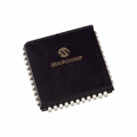
PIC18F442-I/L Microchip Technology, PIC18F442-I/L Datasheet - Page 11

PIC18F442-I/L
Manufacturer Part Number
PIC18F442-I/L
Description
IC MCU FLASH 8KX16 EE A/D 44PLCC
Manufacturer
Microchip Technology
Series
PIC® 18Fr
Datasheets
1.PIC16F616T-ISL.pdf
(8 pages)
2.PIC18F242-ISO.pdf
(332 pages)
3.PIC18F242-ISO.pdf
(14 pages)
4.PIC18F242-ISO.pdf
(16 pages)
5.PIC18F242-ISO.pdf
(16 pages)
6.PIC18F242-ISO.pdf
(14 pages)
7.PIC18LF242-ISO.pdf
(36 pages)
Specifications of PIC18F442-I/L
Core Size
8-Bit
Program Memory Size
16KB (8K x 16)
Core Processor
PIC
Speed
40MHz
Connectivity
I²C, SPI, UART/USART
Peripherals
Brown-out Detect/Reset, LVD, POR, PWM, WDT
Number Of I /o
34
Program Memory Type
FLASH
Eeprom Size
256 x 8
Ram Size
768 x 8
Voltage - Supply (vcc/vdd)
4.2 V ~ 5.5 V
Data Converters
A/D 8x10b
Oscillator Type
External
Operating Temperature
-40°C ~ 85°C
Package / Case
44-PLCC
Controller Family/series
PIC18
No. Of I/o's
34
Eeprom Memory Size
256Byte
Ram Memory Size
768Byte
Cpu Speed
40MHz
No. Of Timers
4
Processor Series
PIC18F
Core
PIC
Data Bus Width
8 bit
Data Ram Size
768 B
Interface Type
MSSP, SPI, I2C, PSP, USART
Maximum Clock Frequency
40 MHz
Number Of Programmable I/os
34
Number Of Timers
1 x 16 bit
Operating Supply Voltage
2 V to 5.5 V
Maximum Operating Temperature
+ 85 C
Mounting Style
SMD/SMT
3rd Party Development Tools
52715-96, 52716-328, 52717-734, 52712-325, EWPIC18
Development Tools By Supplier
PG164130, DV164035, DV244005, DV164005, PG164120, ICE2000, ICE4000, DM163022, DV164136
Minimum Operating Temperature
- 40 C
On-chip Adc
8
Package
44PLCC
Device Core
PIC
Family Name
PIC18
Maximum Speed
40 MHz
Lead Free Status / RoHS Status
Lead free / RoHS Compliant
For Use With
AC164309 - MODULE SKT FOR PM3 44PLCCXLT44L2 - SOCKET TRAN ICE 44PLCC444-1001 - DEMO BOARD FOR PICMICRO MCUDVA16XL441 - ADAPTER DEVICE ICE 44PLCCDV007003 - PROGRAMMER UNIVERSAL PROMATE II
Lead Free Status / Rohs Status
Details
Other names
PIC18F442I/L
Available stocks
Company
Part Number
Manufacturer
Quantity
Price
Company:
Part Number:
PIC18F442-I/L
Manufacturer:
Microchip Technology
Quantity:
10 000
- PIC16F616T-ISL PDF datasheet
- PIC18F242-ISO PDF datasheet #2
- PIC18F242-ISO PDF datasheet #3
- PIC18F242-ISO PDF datasheet #4
- PIC18F242-ISO PDF datasheet #5
- PIC18F242-ISO PDF datasheet #6
- PIC18LF242-ISO PDF datasheet #7
- Current page: 11 of 332
- Download datasheet (6Mb)
FIGURE 1-2:
© 2006 Microchip Technology Inc.
OSC2/CLKO
OSC1/CLKI
T1OSCI
T1OSCO
MCLR
V
DD
Note
Program Memory
Address Latch
(up to 2 Mbytes)
, V
Data Latch
SS
CCP1
Timer0
1: Optional multiplexing of CCP2 input/output with RB3 is enabled by selection of configuration bit.
2: The high order bits of the Direct Address for the RAM are from the BSR register (except for the MOVFF instruction).
3: Many of the general purpose I/O pins are multiplexed with one or more peripheral module functions. The multiplexing combinations
16
are device dependent.
21
21
Generation
Reference
Precision
PIC18F4X2 BLOCK DIAGRAM
Voltage
Timing
4X PLL
Table Latch
Instruction
Decode &
Control
Timer1
CCP2
inc/dec logic
Table Pointer
21
8
Start-up Timer
ROM Latch
Instruction
Programming
Low Voltage
PCLATU
PCU
Program Counter
Register
Power-on
Watchdog
Brown-out
Debugger
Power-up
Oscillator
In-Circuit
31 Level Stack
Reset
Timer
Timer
Reset
Synchronous
8
Serial Port
PCLATH
PCH
Master
Timer2
8
PCL
8
Decode
BIT OP
4
BSR
8
3
Addressable
USART
Timer3
inc/dec
address reach)
12
PRODH
Address Latch
Address<12>
FSR0
FSR1
FSR2
8
Data Latch
Data RAM
logic
WREG
(up to 4K
8 x 8 Multiply
ALU<8>
8
Data Bus<8>
8
12
Bank0, F
PRODL
4
(2)
12
8
Parallel Slave Port
8
8
PORTD
PORTE
PORTA
PORTB
PORTC
PIC18FXX2
A/D Converter
Data EEPROM
RA0/AN0
RA1/AN1
RA2/AN2/V
RA3/AN3/V
RA4/T0CKI
RA5/AN4/SS/LVDIN
RA6
RB3/CCP2
RB4
RB0/INT0
RB1/INT1
RB2/INT2
RB5/PGM
RB6/PCG
RB7/PGD
RC0/T1OSO/T1CKI
RC1/T1OSI/CCP2
RC2/CCP1
RC3/SCK/SCL
RC4/SDI/SDA
RC5/SDO
RC6/TX/CK
RC7/RX/DT
RE0/AN5/RD
RE1/AN6/WR
RE2/AN7/CS
RD0/PSP0
RD1/PSP1
RD2/PSP2
RD3/PSP3
RD4/PSP4
RD5/PSP5
RD6/PSP6
RD7/PSP7
DS39564C-page 9
(1)
REF
REF
-
+
(1)
Related parts for PIC18F442-I/L
Image
Part Number
Description
Manufacturer
Datasheet
Request
R

Part Number:
Description:
IC, 8BIT MCU, PIC18F, 40MHZ, LCC-44
Manufacturer:
Microchip Technology
Datasheet:

Part Number:
Description:
IC, 8BIT MCU, PIC18LF, 40MHZ, PLCC-64
Manufacturer:
Microchip Technology
Datasheet:

Part Number:
Description:
IC, 8BIT MCU, PIC18F, 64MHZ, TQFP-80
Manufacturer:
Microchip Technology
Datasheet:

Part Number:
Description:
MCU, MPU & DSP Development Tools CAN/LIN PICtail Plus Daughter Board
Manufacturer:
Microchip Technology
Datasheet:

Part Number:
Description:
IC, 8BIT MCU, PIC18F, 64MHZ, DIP-40
Manufacturer:
Microchip Technology
Datasheet:

Part Number:
Description:
IC, 8BIT MCU, PIC18LF, 40MHZ, PLCC-64
Manufacturer:
Microchip Technology
Datasheet:

Part Number:
Description:
IC, 8BIT MCU, PIC18F, 64MHZ, TQFP-64
Manufacturer:
Microchip Technology

Part Number:
Description:
IC, 8BIT MCU, PIC18F, 64MHZ, TQFP-80
Manufacturer:
Microchip Technology

Part Number:
Description:
8KB, Flash, 768bytes-RAM, 36I/O, 8-bit Family,nanowatt XLP 40 UQFN 5x5x0.5mm TUB
Manufacturer:
Microchip Technology
Datasheet:

Part Number:
Description:
8KB, Flash, 768bytes-RAM, 36I/O, 8-bit Family,nanowatt XLP 40 UQFN 5x5x0.5mm TUB
Manufacturer:
Microchip Technology

Part Number:
Description:
16KB, Flash, 768bytes-RAM, 36I/O, 8-bit Family,nanowatt XLP 40 UQFN 5x5x0.5mm TU
Manufacturer:
Microchip Technology
Datasheet:

Part Number:
Description:
16KB, Flash, 768bytes-RAM, 36I/O, 8-bit Family,nanowatt XLP 40 UQFN 5x5x0.5mm TU
Manufacturer:
Microchip Technology

Part Number:
Description:
32KB, Flash, 1536bytes-RAM, 36I/O, 8-bit Family,nanowatt XLP 40 UQFN 5x5x0.5mm T
Manufacturer:
Microchip Technology
Datasheet:

Part Number:
Description:
32KB, Flash, 1536bytes-RAM, 36I/O, 8-bit Family,nanowatt XLP 40 UQFN 5x5x0.5mm T
Manufacturer:
Microchip Technology

Part Number:
Description:
64KB, Flash, 3968bytes-RAM, 36I/O, 8-bit Family,nanowatt XLP 40 UQFN 5x5x0.5mm T
Manufacturer:
Microchip Technology
Datasheet:


