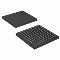
AT91SAM7L64-CU Atmel, AT91SAM7L64-CU Datasheet - Page 166

AT91SAM7L64-CU
Manufacturer Part Number
AT91SAM7L64-CU
Description
MCU ARM7 64K HS FLASH 144-LFBGA
Manufacturer
Atmel
Series
AT91SAMr
Datasheet
1.AT91SAM7L64-CU.pdf
(564 pages)
Specifications of AT91SAM7L64-CU
Core Processor
ARM7
Core Size
16/32-Bit
Speed
36MHz
Connectivity
I²C, SPI, UART/USART
Peripherals
Brown-out Detect/Reset, LCD, POR, PWM, WDT
Number Of I /o
80
Program Memory Size
64KB (64K x 8)
Program Memory Type
FLASH
Ram Size
6K x 8
Voltage - Supply (vcc/vdd)
1.55 V ~ 1.8 V
Data Converters
A/D 4x10b
Oscillator Type
Internal
Operating Temperature
-40°C ~ 85°C
Package / Case
144-LFBGA
Processor Series
AT91SAMx
Core
ARM7TDMI
Data Bus Width
32 bit
Data Ram Size
6 KB
Interface Type
2-Wire, SPI, USART
Maximum Clock Frequency
36 MHz
Number Of Programmable I/os
80
Number Of Timers
3
Maximum Operating Temperature
+ 85 C
Mounting Style
SMD/SMT
3rd Party Development Tools
JTRACE-ARM-2M, MDK-ARM, RL-ARM, ULINK2
Development Tools By Supplier
AT91SAM-ICE, AT91-ISP, AT91SAM7L-EK
Minimum Operating Temperature
- 40 C
On-chip Adc
10 bit, 4 Channel
For Use With
AT91SAM7L-STK - KIT EVAL FOR AT91SAM7LAT91SAM-ICE - EMULATOR FOR AT91 ARM7/ARM9
Lead Free Status / RoHS Status
Lead free / RoHS Compliant
Eeprom Size
-
Lead Free Status / Rohs Status
Details
Available stocks
Company
Part Number
Manufacturer
Quantity
Price
- Current page: 166 of 564
- Download datasheet (9Mb)
20.3
20.3.1
Table 20-16. Signal Description List
166
Signal Name
VDDIO1
VDDIO2
VDDCORE
VDDOUT
VDDINLCD
VDD3V6
VDDLCD
GND
XIN
TST
CLKIN
FWUP
Serial Fast Flash Programming
AT91SAM7L128/64 Preliminary
Device Configuration
Function
I/O Lines Power Supply
I/O Lines Power Supply
Core Power Supply
Voltage Regulator Output
Charge pump input
Charge pump output
LCD voltage input
Ground
Clock Input
Test Mode Select
External clock input used to enter in
FFPI mode
Wake-up pin
The Serial Fast Flash programming interface is based on IEEE Std. 1149.1 “Standard Test
Access Port and Boundary-Scan Architecture”. Refer to this standard for an explanation of terms
used in this chapter and for a description of the TAP controller states.
In this mode, data read/written from/to the embedded Flash of the device are transmitted
through the JTAG interface of the device.
In Serial Fast Flash Programming Mode, the device is in a specific test mode. Only a distinct set
of pins is significant. Other pins must be left unconnected.
Figure 20-5. Serial Programming
0-10MHz
VDDIO1
VDDIO1
GND
TDO
TMS
TCK
TDI
Clocks
Power
Test
TST
CLKIN
FWUP
XIN
Ground
Power
Power
Power
Power
Power
Power
Power
Type
Input
Input
Input
Input
Active
Level
High
High
Low
Comments
Apply externally 2.2V-3.6V (1)
Apply externally 2.2V-3.6V (1)
Apply externally 1.80V-1.95V (1)
Connect to VDDCORE. 2.2 µF
decoupling capacitor needed
Connect to ground
Left unconnected
Connect to VDDIO2
0 to 10MHz (0-VDDIO1 square wave)
Must be connected to VDDIO1
Must be connected to VDDIO1
Must be connected to GND
VDDCORE
VDDIO1
VDDIO2
VDDLCD
GND
VDDINLCD
6257A–ATARM–20-Feb-08
(1)
(1)
Related parts for AT91SAM7L64-CU
Image
Part Number
Description
Manufacturer
Datasheet
Request
R

Part Number:
Description:
KIT EVAL FOR AT91SAM7L
Manufacturer:
Atmel
Datasheet:

Part Number:
Description:
DEV KIT FOR AVR/AVR32
Manufacturer:
Atmel
Datasheet:

Part Number:
Description:
INTERVAL AND WIPE/WASH WIPER CONTROL IC WITH DELAY
Manufacturer:
ATMEL Corporation
Datasheet:

Part Number:
Description:
Low-Voltage Voice-Switched IC for Hands-Free Operation
Manufacturer:
ATMEL Corporation
Datasheet:

Part Number:
Description:
MONOLITHIC INTEGRATED FEATUREPHONE CIRCUIT
Manufacturer:
ATMEL Corporation
Datasheet:

Part Number:
Description:
AM-FM Receiver IC U4255BM-M
Manufacturer:
ATMEL Corporation
Datasheet:

Part Number:
Description:
Monolithic Integrated Feature Phone Circuit
Manufacturer:
ATMEL Corporation
Datasheet:

Part Number:
Description:
Multistandard Video-IF and Quasi Parallel Sound Processing
Manufacturer:
ATMEL Corporation
Datasheet:

Part Number:
Description:
High-performance EE PLD
Manufacturer:
ATMEL Corporation
Datasheet:

Part Number:
Description:
8-bit Flash Microcontroller
Manufacturer:
ATMEL Corporation
Datasheet:

Part Number:
Description:
2-Wire Serial EEPROM
Manufacturer:
ATMEL Corporation
Datasheet:


