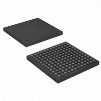
AT91SAM7L64-CU Atmel, AT91SAM7L64-CU Datasheet - Page 323

AT91SAM7L64-CU
Manufacturer Part Number
AT91SAM7L64-CU
Description
MCU ARM7 64K HS FLASH 144-LFBGA
Manufacturer
Atmel
Series
AT91SAMr
Datasheet
1.AT91SAM7L64-CU.pdf
(564 pages)
Specifications of AT91SAM7L64-CU
Core Processor
ARM7
Core Size
16/32-Bit
Speed
36MHz
Connectivity
I²C, SPI, UART/USART
Peripherals
Brown-out Detect/Reset, LCD, POR, PWM, WDT
Number Of I /o
80
Program Memory Size
64KB (64K x 8)
Program Memory Type
FLASH
Ram Size
6K x 8
Voltage - Supply (vcc/vdd)
1.55 V ~ 1.8 V
Data Converters
A/D 4x10b
Oscillator Type
Internal
Operating Temperature
-40°C ~ 85°C
Package / Case
144-LFBGA
Processor Series
AT91SAMx
Core
ARM7TDMI
Data Bus Width
32 bit
Data Ram Size
6 KB
Interface Type
2-Wire, SPI, USART
Maximum Clock Frequency
36 MHz
Number Of Programmable I/os
80
Number Of Timers
3
Maximum Operating Temperature
+ 85 C
Mounting Style
SMD/SMT
3rd Party Development Tools
JTRACE-ARM-2M, MDK-ARM, RL-ARM, ULINK2
Development Tools By Supplier
AT91SAM-ICE, AT91-ISP, AT91SAM7L-EK
Minimum Operating Temperature
- 40 C
On-chip Adc
10 bit, 4 Channel
For Use With
AT91SAM7L-STK - KIT EVAL FOR AT91SAM7LAT91SAM-ICE - EMULATOR FOR AT91 ARM7/ARM9
Lead Free Status / RoHS Status
Lead free / RoHS Compliant
Eeprom Size
-
Lead Free Status / Rohs Status
Details
Available stocks
Company
Part Number
Manufacturer
Quantity
Price
- Current page: 323 of 564
- Download datasheet (9Mb)
29.7
29.7.1
29.7.2
29.7.3
29.7.4
6257A–ATARM–20-Feb-08
Master Mode
Definition
Application Block Diagram
Programming Master Mode
Master Transmitter Mode
The Master is the device that starts a transfer, generates a clock and stops it.
Figure 29-5. Master Mode Typical Application Block Diagram
The following registers have to be programmed before entering Master mode:
After the master initiates a Start condition when writing into the Transmit Holding Register,
TWI_THR, it sends a 7-bit slave address, configured in the Master Mode register (DADR in
TWI_MMR), to notify the slave device. The bit following the slave address indicates the transfer
direction, 0 in this case (MREAD = 0 in TWI_MMR).
The TWI transfers require the slave to acknowledge each received byte. During the acknowl-
edge clock pulse (9th pulse), the master releases the data line (HIGH), enabling the slave to pull
it down in order to generate the acknowledge. The master polls the data line during this clock
pulse and sets the Not Acknowledge bit (NACK) in the status register if the slave does not
acknowledge the byte. As with the other status bits, an interrupt can be generated if enabled in
the interrupt enable register (TWI_IER). If the slave acknowledges the byte, the data written in
the TWI_THR, is then shifted in the internal shifter and transferred. When an acknowledge is
detected, the TXRDY bit is set until a new write in the TWI_THR.
1. DADR (+ IADRSZ + IADR if a 10 bit device is addressed): The device address is used
2. CKDIV + CHDIV + CLDIV: Clock Waveform.
3. SVDIS: Disable the slave mode.
4. MSEN: Enable the master mode.
Rp: Pull up value as given by the I²C Standard
Host with
Interface
to access slave devices in read or write mode.
TWI
TWD
TWCK
Serial EEPROM
Atmel TWI
Slave 1
AT91SAM7L128/64 Preliminary
I²C RTC
Slave 2
Controller
I²C LCD
Slave 3
I²C Temp.
Sensor
Slave 4
Rp
Rp
VDD
323
Related parts for AT91SAM7L64-CU
Image
Part Number
Description
Manufacturer
Datasheet
Request
R

Part Number:
Description:
KIT EVAL FOR AT91SAM7L
Manufacturer:
Atmel
Datasheet:

Part Number:
Description:
DEV KIT FOR AVR/AVR32
Manufacturer:
Atmel
Datasheet:

Part Number:
Description:
INTERVAL AND WIPE/WASH WIPER CONTROL IC WITH DELAY
Manufacturer:
ATMEL Corporation
Datasheet:

Part Number:
Description:
Low-Voltage Voice-Switched IC for Hands-Free Operation
Manufacturer:
ATMEL Corporation
Datasheet:

Part Number:
Description:
MONOLITHIC INTEGRATED FEATUREPHONE CIRCUIT
Manufacturer:
ATMEL Corporation
Datasheet:

Part Number:
Description:
AM-FM Receiver IC U4255BM-M
Manufacturer:
ATMEL Corporation
Datasheet:

Part Number:
Description:
Monolithic Integrated Feature Phone Circuit
Manufacturer:
ATMEL Corporation
Datasheet:

Part Number:
Description:
Multistandard Video-IF and Quasi Parallel Sound Processing
Manufacturer:
ATMEL Corporation
Datasheet:

Part Number:
Description:
High-performance EE PLD
Manufacturer:
ATMEL Corporation
Datasheet:

Part Number:
Description:
8-bit Flash Microcontroller
Manufacturer:
ATMEL Corporation
Datasheet:

Part Number:
Description:
2-Wire Serial EEPROM
Manufacturer:
ATMEL Corporation
Datasheet:


