P87C660X2BBD,157 NXP Semiconductors, P87C660X2BBD,157 Datasheet - Page 7
P87C660X2BBD,157
Manufacturer Part Number
P87C660X2BBD,157
Description
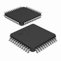
IC 80C51 MCU 16K OTP 44-LQFP
Manufacturer
NXP Semiconductors
Series
87Cr
Datasheet
1.P87C660X2BBD157.pdf
(102 pages)
Specifications of P87C660X2BBD,157
Core Processor
8051
Core Size
8-Bit
Speed
33MHz
Connectivity
EBI/EMI, I²C, UART/USART
Peripherals
POR, PWM, WDT
Number Of I /o
32
Program Memory Size
16KB (16K x 8)
Program Memory Type
OTP
Ram Size
512 x 8
Voltage - Supply (vcc/vdd)
2.7 V ~ 5.5 V
Oscillator Type
Internal
Operating Temperature
0°C ~ 70°C
Package / Case
44-LQFP
Processor Series
P87C6x
Core
80C51
Data Bus Width
8 bit
Data Ram Size
512 B
Interface Type
I2C, UART
Maximum Clock Frequency
16 MHz, 33 MHz
Number Of Programmable I/os
32
Number Of Timers
3
Operating Supply Voltage
2.7 V to 5.5 V
Maximum Operating Temperature
+ 70 C
Mounting Style
SMD/SMT
3rd Party Development Tools
PK51, CA51, A51, ULINK2
Minimum Operating Temperature
0 C
Lead Free Status / RoHS Status
Lead free / RoHS Compliant
Eeprom Size
-
Data Converters
-
Lead Free Status / Rohs Status
Details
Other names
568-3204
935273061157
P87C660X2BBD
935273061157
P87C660X2BBD
Available stocks
Company
Part Number
Manufacturer
Quantity
Price
Company:

Part Number:
P87C660X2BBD,157
Manufacturer:
NXP Semiconductors
Quantity:
10 000


Philips Semiconductors
PIN DESCRIPTIONS
2003 Oct 02
V
V
V
V
P0.0–0.7
P1.0–P1.7
P2.0–P2.7
P3.0–P3.7
RST
SCL1
SDA1
MNEMONIC
MNEMONIC
SS1
SS2
SS3
CC
80C51 8-bit microcontroller family
RAM, low voltage (2.7 to 5.5 V), low power, high speed (30/33
MHz), two 400KB I
2
2
2
2
2
PLCC
43–36
24–31
13–19
2–9
PIN NUMBER
11,
22
34
12
44
13
14
15
16
17
18
19
10
23
11
2
3
4
5
6
7
8
9
1
2
C interfaces
5, 7–13
40–44,
37–30
18–25
LQFP
1–3
16
28
38
40
41
42
43
44
10
11
12
13
17
39
6
1
2
3
5
7
8
9
4
TYPE
TYPE
I/O
I/O
I/O
I/O
I/O
I/O
I/O
I/O
I/O
I/O
I/O
I/O
O
O
O
I
I
I
I
I
I
I
I
I
I
I
I
16 KB OTP/ROM, 512B
and data memory. In this application, it uses strong internal pull-ups when emitting 1s.
Ground: 0 V reference.
Ground: Additional ground pin (may be left open).
Ground: Additional ground pin (may be left open).
Power Supply: This is the power supply voltage for normal, idle, and power-down
operation.
Port 0: Port 0 is an open-drain, bidirectional I/O port. Port 0 pins that have 1s
written to them float and can be used as high-impedance inputs. Port 0 is also the
multiplexed low-order address and data bus during accesses to external program
Port 1: Port 1 is an 8-bit bidirectional I/O port with internal pull-ups on all pins.
Port 1 pins that have 1s written to them are pulled HIGH by the internal pull-ups and
can be used as inputs. As inputs, port 1 pins that are externally pulled LOW will
source current because of the internal pull-ups. (See DC Electrical Characteristics:
I
Alternate functions for P8xC660X2/661X2 Port 1 include:
Port 2: Port 2 is an 8-bit bidirectional I/O port with internal pull-ups. Port 2 pins that
have 1s written to them are pulled HIGH by the internal pull-ups and can be used
as inputs. As inputs, port 2 pins that are externally being pulled LOW will source
current because of the internal pull-ups. (See DC Electrical Characteristics: I
Port 2 emits the high-order address byte during fetches from external program
memory and during accesses to external data memory that use 16-bit addresses
(MOVX @DPTR). In this application, it uses strong internal pull-ups when emitting
1s. During accesses to external data memory that use 8-bit addresses (MOV @Ri),
port 2 emits the contents of the P2 special function register.
Port 3: Port 3 is an 8-bit bidirectional I/O port with internal pull-ups. Port 3 pins that
have 1s written to them are pulled HIGH by the internal pull-ups and can be used
as inputs. As inputs, port 3 pins that are externally being pulled LOW will source
current because of the pull-ups. (See DC Electrical Characteristics: I
serves the special features of the P8xC660X2/661X2, as listed below:
Reset: A HIGH on this pin for two machine cycles while the oscillator is running,
resets the device. An internal resistor to V
an external capacitor to V
Second I
Second I
IL
).
T2 (P1.0): Timer/Counter 2 external count input/Clockout (see Programmable
Clock-Out)
T2EX (P1.1): Timer/Counter 2 Reload/Capture/Direction Control
ECI (P1.2): External Clock Input to the PCA
CEX0 (P1.3): Capture/Compare External I/O for PCA module 0
CEX1 (P1.4): Capture/Compare External I/O for PCA module 1
CEX2 (P1.5): Capture/Compare External I/O for PCA module 2
SCL (P1.6): I
SCL (P1.7): I
RxD (P3.0): Serial input port
TxD (P3.1): Serial output port
INT0 (P3.2): External interrupt 0
INT1 (P3.3): External interrupt 1
CEX3/T0 (P3.4): Timer 0 external input; capture/compare external I/O for PCA
module 3
CEX4/T1 (P3.5): Timer 1 external input; capture/compare external I/O for PCA
module 4
WR (P3.6): External data memory write strobe
RD (P3.7): External data memory read strobe
2
2
C bus clock line (open drain) (P8xC661X2)
C bus data line (open drain) (P8xC661X2)
2
2
C bus clock line (open drain)
C bus data line (open drain)
7
CC
.
NAME AND FUNCTION
NAME AND FUNCTION
SS
permits a power-on reset using only
P8xC660X2/661X2
IL
). Port 3 also
IL
).
Product data
Related parts for P87C660X2BBD,157
Image
Part Number
Description
Manufacturer
Datasheet
Request
R

Part Number:
Description:
80C51 8-bit microcontroller family
Manufacturer:
PHILIPS [NXP Semiconductors]
Datasheet:

Part Number:
Description:
NXP Semiconductors designed the LPC2420/2460 microcontroller around a 16-bit/32-bitARM7TDMI-S CPU core with real-time debug interfaces that include both JTAG andembedded trace
Manufacturer:
NXP Semiconductors
Datasheet:

Part Number:
Description:
NXP Semiconductors designed the LPC2458 microcontroller around a 16-bit/32-bitARM7TDMI-S CPU core with real-time debug interfaces that include both JTAG andembedded trace
Manufacturer:
NXP Semiconductors
Datasheet:
Part Number:
Description:
NXP Semiconductors designed the LPC2468 microcontroller around a 16-bit/32-bitARM7TDMI-S CPU core with real-time debug interfaces that include both JTAG andembedded trace
Manufacturer:
NXP Semiconductors
Datasheet:
Part Number:
Description:
NXP Semiconductors designed the LPC2470 microcontroller, powered by theARM7TDMI-S core, to be a highly integrated microcontroller for a wide range ofapplications that require advanced communications and high quality graphic displays
Manufacturer:
NXP Semiconductors
Datasheet:
Part Number:
Description:
NXP Semiconductors designed the LPC2478 microcontroller, powered by theARM7TDMI-S core, to be a highly integrated microcontroller for a wide range ofapplications that require advanced communications and high quality graphic displays
Manufacturer:
NXP Semiconductors
Datasheet:
Part Number:
Description:
The Philips Semiconductors XA (eXtended Architecture) family of 16-bit single-chip microcontrollers is powerful enough to easily handle the requirements of high performance embedded applications, yet inexpensive enough to compete in the market for hi
Manufacturer:
NXP Semiconductors
Datasheet:
Part Number:
Description:
The XA-S3 device is a member of Philips Semiconductors? XA(eXtended Architecture) family of high performance 16-bitsingle-chip microcontrollers
Manufacturer:
NXP Semiconductors
Datasheet:

Part Number:
Description:
The NXP BlueStreak LH75401/LH75411 family consists of two low-cost 16/32-bit System-on-Chip (SoC) devices
Manufacturer:
NXP Semiconductors
Datasheet:
Part Number:
Description:
The NXP LPC3130/3131 combine an 180 MHz ARM926EJ-S CPU core, high-speed USB2
Manufacturer:
NXP Semiconductors
Datasheet:
Part Number:
Description:
The NXP LPC3141 combine a 270 MHz ARM926EJ-S CPU core, High-speed USB 2
Manufacturer:
NXP Semiconductors
Part Number:
Description:
The NXP LPC3143 combine a 270 MHz ARM926EJ-S CPU core, High-speed USB 2
Manufacturer:
NXP Semiconductors

Part Number:
Description:
The NXP LPC3152 combines an 180 MHz ARM926EJ-S CPU core, High-speed USB 2
Manufacturer:
NXP Semiconductors
Part Number:
Description:
The NXP LPC3154 combines an 180 MHz ARM926EJ-S CPU core, High-speed USB 2
Manufacturer:
NXP Semiconductors