P80C552EBA/08,512 NXP Semiconductors, P80C552EBA/08,512 Datasheet - Page 7
P80C552EBA/08,512
Manufacturer Part Number
P80C552EBA/08,512
Description
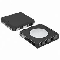
IC 80C51 MCU 8BIT ROMLESS 68PLCC
Manufacturer
NXP Semiconductors
Series
80Cr
Datasheet
1.P80C552EBA08512.pdf
(23 pages)
Specifications of P80C552EBA/08,512
Program Memory Type
ROMless
Package / Case
68-PLCC
Core Processor
8051
Core Size
8-Bit
Speed
16MHz
Connectivity
EBI/EMI, I²C, UART/USART
Peripherals
POR, PWM, WDT
Number Of I /o
40
Ram Size
256 x 8
Voltage - Supply (vcc/vdd)
4.5 V ~ 5.5 V
Data Converters
A/D 8x10b
Oscillator Type
Internal
Operating Temperature
0°C ~ 70°C
Processor Series
P80C5x
Core
80C51
Data Bus Width
8 bit
Data Ram Size
256 B
Interface Type
I2C/UART
Maximum Clock Frequency
16 MHz
Number Of Programmable I/os
40
Number Of Timers
3
Operating Supply Voltage
4.5 V to 5.5 V
Maximum Operating Temperature
+ 70 C
Mounting Style
SMD/SMT
3rd Party Development Tools
PK51, CA51, A51, ULINK2
Minimum Operating Temperature
0 C
On-chip Adc
8-ch x 10-bit
Lead Free Status / RoHS Status
Lead free / RoHS Compliant
Eeprom Size
-
Program Memory Size
-
Lead Free Status / Rohs Status
Lead free / RoHS Compliant
Other names
568-1235-5
935262803512
P80C552EBA
935262803512
P80C552EBA
Available stocks
Company
Part Number
Manufacturer
Quantity
Price
Company:

Part Number:
P80C552EBA/08,512
Manufacturer:
NXP Semiconductors
Quantity:
10 000


Philips Semiconductors
PIN DESCRIPTION
2002 Sep 03
V
STADC
PWM0
PWM1
EW
P0.0-P0.7
P1.0-P1.7
P2.0-P2.7
P3.0-P3.7
P4.0-P4.7
P5.0-P5.7
RST
XTAL1
XTAL2
MNEMONIC
DD
Single-chip 8-bit microcontroller with 10-bit A/D,
capture/compare timer, high-speed outputs, PWM
68-62,
PLCC
13, 14
57-50
16-23
16-21
22-23
16-19
39-46
24-31
7-14
7-12
20
21
22
23
24
25
26
27
28
29
30
31
15
35
34
2
3
4
5
6
1
PIN NO.
80, 1-2
80, 1-2
38-42,
18-20,
71-64,
58-51
10-17
10-15
16-17
10-13
45-47
23-27
QFP
7, 8
4-8
4-6
72
74
75
76
77
14
15
16
17
18
19
20
23
24
25
26
27
32
31
9
TYPE
I/O
I/O
I/O
I/O
I/O
I/O
I/O
I/O
I/O
I/O
O
O
O
O
O
I
I
I
I
I
I
I
I
CMT0, CMT1 (P4.6, P4.7): Timer T2 compare and toggle outputs on a match with timer T2.
Digital Power Supply: +5 V power supply pin during normal operation, idle and
power-down mode.
Start ADC Operation: Input starting analog to digital conversion (ADC operation can also
be started by software). This pin must not float.
Pulse Width Modulation: Output 0.
Pulse Width Modulation: Output 1.
Enable Watchdog Timer: Enable for T3 watchdog timer and disable power-down mode.
This pin must not float.
Port 0: Port 0 is an 8-bit open-drain bidirectional I/O port. Port 0 pins that have 1s written
to them float and can be used as high-impedance inputs. Port 0 is also the multiplexed
low-order address and data bus during accesses to external program and data memory. In
this application it uses strong internal pull-ups when emitting 1s.
Port 1: 8-bit I/O port. Alternate functions include:
(P1.0-P1.5): Quasi-bidirectional port pins.
(P1.6, P1.7): Open drain port pins.
CT0I-CT3I (P1.0-P1.3): Capture timer input signals for timer T2.
T2 (P1.4): T2 event input.
RT2 (P1.5): T2 timer reset signal. Rising edge triggered.
SCL (P1.6): Serial port clock line I
SDA (P1.7): Serial port data line I
Port 1 is also used to input the lower order address byte during EPROM programming and
verification. A0 is on P1.0, etc.
Port 2: 8-bit quasi-bidirectional I/O port.
Alternate function: High-order address byte for external memory (A08-A15).
Port 3: 8-bit quasi-bidirectional I/O port. Alternate functions include:
RxD(P3.0): Serial input port.
TxD (P3.1): Serial output port.
INT0 (P3.2): External interrupt.
INT1 (P3.3): External interrupt.
T0 (P3.4): Timer 0 external input.
T1 (P3.5): Timer 1 external input.
WR (P3.6): External data memory write strobe.
RD (P3.7): External data memory read strobe.
Port 4: 8-bit quasi-bidirectional I/O port. Alternate functions include:
CMSR0-CMSR5 (P4.0-P4.5): Timer T2 compare and set/reset outputs on a match with
timer T2.
Port 5: 8-bit input port.
ADC0-ADC7 (P5.0-P5.7): Alternate function: Eight input channels to ADC.
Reset: Input to reset the 8XC552. It also provides a reset pulse as output when timer T3
overflows.
Crystal Input 1: Input to the inverting amplifier that forms the oscillator, and input to the
internal clock generator. Receives the external clock signal when an external oscillator is
used.
Crystal Input 2: Output of the inverting amplifier that forms the oscillator. Left open-circuit
when an external clock is used.
7
NAME AND FUNCTION
2
2
C-bus.
C-bus.
80C552/83C552
Product data
Related parts for P80C552EBA/08,512
Image
Part Number
Description
Manufacturer
Datasheet
Request
R

Part Number:
Description:
357-036-542-201 CARDEDGE 36POS DL .156 BLK LOPRO
Manufacturer:
NXP Semiconductors
Datasheet:
Part Number:
Description:
IC 80C51 MCU 8BIT ROMLESS 68PLCC
Manufacturer:
NXP Semiconductors
Datasheet:
Part Number:
Description:
NXP Semiconductors designed the LPC2420/2460 microcontroller around a 16-bit/32-bitARM7TDMI-S CPU core with real-time debug interfaces that include both JTAG andembedded trace
Manufacturer:
NXP Semiconductors
Datasheet:

Part Number:
Description:
NXP Semiconductors designed the LPC2458 microcontroller around a 16-bit/32-bitARM7TDMI-S CPU core with real-time debug interfaces that include both JTAG andembedded trace
Manufacturer:
NXP Semiconductors
Datasheet:
Part Number:
Description:
NXP Semiconductors designed the LPC2468 microcontroller around a 16-bit/32-bitARM7TDMI-S CPU core with real-time debug interfaces that include both JTAG andembedded trace
Manufacturer:
NXP Semiconductors
Datasheet:
Part Number:
Description:
NXP Semiconductors designed the LPC2470 microcontroller, powered by theARM7TDMI-S core, to be a highly integrated microcontroller for a wide range ofapplications that require advanced communications and high quality graphic displays
Manufacturer:
NXP Semiconductors
Datasheet:
Part Number:
Description:
NXP Semiconductors designed the LPC2478 microcontroller, powered by theARM7TDMI-S core, to be a highly integrated microcontroller for a wide range ofapplications that require advanced communications and high quality graphic displays
Manufacturer:
NXP Semiconductors
Datasheet:
Part Number:
Description:
The Philips Semiconductors XA (eXtended Architecture) family of 16-bit single-chip microcontrollers is powerful enough to easily handle the requirements of high performance embedded applications, yet inexpensive enough to compete in the market for hi
Manufacturer:
NXP Semiconductors
Datasheet:
Part Number:
Description:
The XA-S3 device is a member of Philips Semiconductors? XA(eXtended Architecture) family of high performance 16-bitsingle-chip microcontrollers
Manufacturer:
NXP Semiconductors
Datasheet:

Part Number:
Description:
The NXP BlueStreak LH75401/LH75411 family consists of two low-cost 16/32-bit System-on-Chip (SoC) devices
Manufacturer:
NXP Semiconductors
Datasheet:
Part Number:
Description:
The NXP LPC3130/3131 combine an 180 MHz ARM926EJ-S CPU core, high-speed USB2
Manufacturer:
NXP Semiconductors
Datasheet:
Part Number:
Description:
The NXP LPC3141 combine a 270 MHz ARM926EJ-S CPU core, High-speed USB 2
Manufacturer:
NXP Semiconductors
Part Number:
Description:
The NXP LPC3143 combine a 270 MHz ARM926EJ-S CPU core, High-speed USB 2
Manufacturer:
NXP Semiconductors

Part Number:
Description:
The NXP LPC3152 combines an 180 MHz ARM926EJ-S CPU core, High-speed USB 2
Manufacturer:
NXP Semiconductors