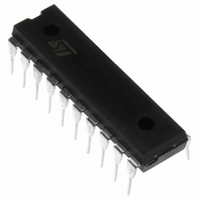
ST7FLITE29F2B6 STMicroelectronics, ST7FLITE29F2B6 Datasheet - Page 33

ST7FLITE29F2B6
Manufacturer Part Number
ST7FLITE29F2B6
Description
IC MCU 8BIT 8K FLASH 20DIP
Manufacturer
STMicroelectronics
Series
ST7r
Datasheet
1.ST7FLITE20F2B6.pdf
(133 pages)
Specifications of ST7FLITE29F2B6
Core Processor
ST7
Core Size
8-Bit
Speed
8MHz
Connectivity
SPI
Peripherals
LVD, POR, PWM, WDT
Number Of I /o
15
Program Memory Size
8KB (8K x 8)
Program Memory Type
FLASH
Eeprom Size
256 x 8
Ram Size
384 x 8
Voltage - Supply (vcc/vdd)
2.4 V ~ 5.5 V
Data Converters
A/D 7x10b
Oscillator Type
Internal
Operating Temperature
-40°C ~ 85°C
Package / Case
20-DIP (0.300", 7.62mm)
Processor Series
ST7FLITE2x
Core
ST7
Data Bus Width
8 bit
Data Ram Size
384 B
Interface Type
SPI
Maximum Clock Frequency
8 MHz
Number Of Programmable I/os
15
Number Of Timers
4 bit
Operating Supply Voltage
2.4 V to 5.5 V
Maximum Operating Temperature
+ 85 C
Mounting Style
Through Hole
Development Tools By Supplier
ST7FLIT2-COS/COM, ST7FLITE-SK/RAIS, ST7MDT10-DVP3, ST7MDT10-EMU3, STX-RLINK
Minimum Operating Temperature
- 40 C
On-chip Adc
13 bit
For Use With
497-5858 - EVAL BOARD PLAYBACK ST7FLITE497-5049 - KIT STARTER RAISONANCE ST7FLITE497-5046 - KIT TOOL FOR ST7/UPSD/STR7 MCU
Lead Free Status / RoHS Status
Lead free / RoHS Compliant
Other names
497-2134-5
Available stocks
Company
Part Number
Manufacturer
Quantity
Price
Part Number:
ST7FLITE29F2B6
Manufacturer:
ST
Quantity:
20 000
SYSTEM INTEGRITY MANAGEMENT (Cont’d)
7.6.4 Register Description
SYSTEM INTEGRITY (SI) CONTROL/STATUS REGISTER (SICSR)
Read/Write
Reset Value: 0000 0xx0 (0xh)
Bit 7:5 = Reserved, must be kept cleared.
Bit 4 = WDGRF Watchdog reset flag
This bit indicates that the last Reset was generat-
ed by the Watchdog peripheral. It is set by hard-
ware (watchdog reset) and cleared by software
(writing zero) or an LVD Reset (to ensure a stable
cleared state of the WDGRF flag when CPU
starts).
Combined with the LVDRF flag information, the
flag description is given by the following table.
Bit 3 = LOCKED PLL Locked Flag
This bit is set and cleared by hardware. It is set au-
tomatically when the PLL reaches its operating fre-
quency.
0: PLL not locked
1: PLL locked
7
0
0
External RESET pin
RESET Sources
Watchdog
0
LVD
WDG
RF
LOCKED LVDRF AVDF AVDIE
LVDRF
0
0
1
WDGRF
X
1
0
0
Bit 2 = LVDRF LVD reset flag
This bit indicates that the last Reset was generat-
ed by the LVD block. It is set by hardware (LVD re-
set) and cleared by software (by reading). When
the LVD is disabled by OPTION BYTE, the LVDRF
bit value is undefined.
Bit 1 = AVDF Voltage Detector flag
This read-only bit is set and cleared by hardware.
If the AVDIE bit is set, an interrupt request is gen-
erated when the AVDF bit is set. Refer to
19
0: V
1: V
Bit 0 = AVDIE Voltage Detector interrupt enable
This bit is set and cleared by software. It enables
an interrupt to be generated when the AVDF flag is
set. The pending interrupt information is automati-
cally cleared when software enters the AVD inter-
rupt routine.
0: AVD interrupt disabled
1: AVD interrupt enabled
Application notes
The LVDRF flag is not cleared when another RE-
SET type occurs (external or watchdog), the
LVDRF flag remains set to keep trace of the origi-
nal failure.
In this case, a watchdog reset can be detected by
software while an external reset can not.
and to
DD
DD
over AVD threshold
under AVD threshold
Section 7.6.2.1
for additional details.
ST7LITE2
Figure
33/133
1


