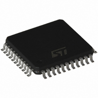
ST72F325J7T6 STMicroelectronics, ST72F325J7T6 Datasheet - Page 96

ST72F325J7T6
Manufacturer Part Number
ST72F325J7T6
Description
IC MCU 8BIT 48K FLASH 44-LQFP
Manufacturer
STMicroelectronics
Series
ST7r
Datasheet
1.ST72F325K6T6.pdf
(197 pages)
Specifications of ST72F325J7T6
Core Processor
ST7
Core Size
8-Bit
Speed
8MHz
Connectivity
I²C, SCI, SPI
Peripherals
LVD, POR, PWM, WDT
Number Of I /o
32
Program Memory Size
48KB (48K x 8)
Program Memory Type
FLASH
Ram Size
1.5K x 8
Voltage - Supply (vcc/vdd)
3.8 V ~ 5.5 V
Data Converters
A/D 16x10b
Oscillator Type
Internal
Operating Temperature
-40°C ~ 85°C
Package / Case
44-LQFP
Processor Series
ST72F3x
Core
ST7
Data Bus Width
8 bit
Data Ram Size
1.5 KB
Interface Type
I2C, SCI, SPI
Maximum Clock Frequency
8 MHz
Number Of Programmable I/os
48
Number Of Timers
2
Maximum Operating Temperature
+ 85 C
Mounting Style
SMD/SMT
Development Tools By Supplier
ST7232X-EVAL, ST7232X-SK/RAIS, ST72325-D/RAIS, ST7MDT20-DVP3, ST7MDT20J-EMU3, ST7MDT20M-EMU3, STX-RLINK
Minimum Operating Temperature
- 40 C
On-chip Adc
10 bit, 16 Channel
A/d Bit Size
10 bit
A/d Channels Available
16
Height
1.4 mm
Length
10 mm
Supply Voltage (max)
5.5 V
Supply Voltage (min)
3.8 V, 4.5 V
Width
10 mm
For Use With
497-5046 - KIT TOOL FOR ST7/UPSD/STR7 MCU
Lead Free Status / RoHS Status
Lead free / RoHS Compliant
Eeprom Size
-
Lead Free Status / Rohs Status
Details
Other names
497-8243
ST72F325J7T6
ST72F325J7T6
Available stocks
Company
Part Number
Manufacturer
Quantity
Price
Company:
Part Number:
ST72F325J7T6
Manufacturer:
STMicroelectronics
Quantity:
10 000
Company:
Part Number:
ST72F325J7T6TR
Manufacturer:
STMicroelectronics
Quantity:
10 000
ST72325xx
SERIAL PERIPHERAL INTERFACE (Cont’d)
10.5.4 Clock Phase and Clock Polarity
Four possible timing relationships may be chosen
by software, using the CPOL and CPHA bits (See
Figure
Note: The idle state of SCK must correspond to
the polarity selected in the SPICSR register (by
pulling up SCK if CPOL=1 or pulling down SCK if
CPOL=0).
The combination of the CPOL clock polarity and
CPHA (clock phase) bits selects the data capture
clock edge
Figure 60. Data Clock Timing Diagram
96/197
(from slave)
(from slave)
60).
(to slave)
(to slave)
(from master)
(from master)
MISO
MOSI
CAPTURE STROBE
SCK
(CPOL = 1)
SCK
(CPOL = 0)
MISO
MOSI
SS
CAPTURE STROBE
SCK
(CPOL = 1)
SCK
(CPOL = 0)
SS
Note: This figure should not be used as a replacement for parametric information.
Refer to the Electrical Characteristics chapter.
MSBit
MSBit
MSBit
MSBit
Bit 6
Bit 6
Bit 6
Bit 6
Bit 5
Bit 5
Bit 5
Bit 5
CPHA =0
CPHA =1
Bit 4
Bit 4
Bit 4
Bit 4
Figure
combinations of the CPHA and CPOL bits. The di-
agram may be interpreted as a master or slave
timing diagram where the SCK pin, the MISO pin,
the MOSI pin are directly connected between the
master and the slave device.
Note: If CPOL is changed at the communication
byte boundaries, the SPI must be disabled by re-
setting the SPE bit.
Bit3
Bit3
Bit3
Bit3
60, shows an SPI transfer with the four
Bit 2
Bit 2
Bit 2
Bit 2
Bit 1
Bit 1
Bit 1
Bit 1
LSBit
LSBit
LSBit
LSBit


