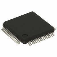
ST72F321BAR9T6 STMicroelectronics, ST72F321BAR9T6 Datasheet - Page 116

ST72F321BAR9T6
Manufacturer Part Number
ST72F321BAR9T6
Description
MCU 8BIT 60KB FLASH/ROM 64-LQFP
Manufacturer
STMicroelectronics
Series
ST7r
Datasheet
1.ST72F321BK6T6.pdf
(187 pages)
Specifications of ST72F321BAR9T6
Core Processor
ST7
Core Size
8-Bit
Speed
8MHz
Connectivity
I²C, SCI, SPI
Peripherals
LVD, POR, PWM, WDT
Number Of I /o
48
Program Memory Size
60KB (60K x 8)
Program Memory Type
FLASH
Ram Size
2K x 8
Voltage - Supply (vcc/vdd)
3.8 V ~ 5.5 V
Data Converters
A/D 16x10b
Oscillator Type
Internal
Operating Temperature
-40°C ~ 85°C
Package / Case
64-LQFP
Processor Series
ST72F3x
Core
ST7
Data Bus Width
8 bit
Data Ram Size
2 KB
Interface Type
I2C, SCI, SPI
Maximum Clock Frequency
8 MHz
Number Of Programmable I/os
48
Number Of Timers
2
Maximum Operating Temperature
+ 85 C
Mounting Style
SMD/SMT
Development Tools By Supplier
ST7232X-EVAL, ST7232X-SK/RAIS, ST72321B-D/RAIS, ST7MDT20-DVP3, ST7MDT20J-EMU3, ST7MDT20M-EMU3, STX-RLINK
Minimum Operating Temperature
- 40 C
On-chip Adc
10 bit, 16 Channel
For Use With
497-5046 - KIT TOOL FOR ST7/UPSD/STR7 MCU
Lead Free Status / RoHS Status
Lead free / RoHS Compliant
Eeprom Size
-
Lead Free Status / Rohs Status
Details
Other names
497-5583
Available stocks
Company
Part Number
Manufacturer
Quantity
Price
Company:
Part Number:
ST72F321BAR9T6
Manufacturer:
STMicroelectronics
Quantity:
32
Company:
Part Number:
ST72F321BAR9T6
Manufacturer:
STMicroelectronics
Quantity:
10 000
Part Number:
ST72F321BAR9T6
Manufacturer:
ST
Quantity:
20 000
ST72321BRx, ST72321BARx ST72321BJx, ST72321BKx
I
Acknowledge may be enabled and disabled by
software.
The I
dress can be selected by software.
The speed of the I
between Standard (up to 100KHz) and Fast I
(up to 400KHz).
SDA/SCL Line Control
Transmitter mode: the interface holds the clock
line low before transmission to wait for the micro-
controller to write the byte in the Data Register.
Receiver mode: the interface holds the clock line
low after reception to wait for the microcontroller to
read the byte in the Data Register.
Figure 66. I
116/187
2
C BUS INTERFACE (Cont’d)
SCL or SCLI
SDA or SDAI
2
C interface address and/or general call ad-
2
C Interface Block Diagram
2
C interface may be selected
CLOCK CONTROL
CLOCK CONTROL REGISTER (CCR)
DATA CONTROL
STATUS REGISTER 1 (SR1)
STATUS REGISTER 2 (SR2)
CONTROL REGISTER (CR)
2
C
The SCL frequency (F
grammable clock divider which depends on the
I
When the I
ports must be configured as floating inputs. In this
case, the value of the external pull-up resistor
used depends on the application.
When the I
ports revert to being standard I/O port pins.
2
OWN ADDRESS REGISTER 1 (OAR1)
OWN ADDRESS REGISTER 2 (OAR2)
C bus mode.
DATA SHIFT REGISTER
DATA REGISTER (DR)
CONTROL LOGIC
COMPARATOR
INTERRUPT
2
2
C cell is disabled, the SDA and SCL
C cell is enabled, the SDA and SCL
scl
) is controlled by a pro-


