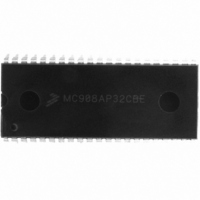
MC908AP32CBE Freescale Semiconductor, MC908AP32CBE Datasheet - Page 125

MC908AP32CBE
Manufacturer Part Number
MC908AP32CBE
Description
IC MCU 32K FLASH 8MHZ 42DIP
Manufacturer
Freescale Semiconductor
Series
HC08r
Specifications of MC908AP32CBE
Core Processor
HC08
Core Size
8-Bit
Speed
8MHz
Connectivity
I²C, IRSCI, SCI, SPI
Peripherals
LED, LVD, POR, PWM
Number Of I /o
30
Program Memory Size
32KB (32K x 8)
Program Memory Type
FLASH
Ram Size
2K x 8
Voltage - Supply (vcc/vdd)
2.7 V ~ 5.5 V
Data Converters
A/D 8x10b
Oscillator Type
Internal
Operating Temperature
-40°C ~ 85°C
Package / Case
42-DIP (0.600", 15.24mm)
Controller Family/series
HC08
No. Of I/o's
30
Ram Memory Size
2KB
Cpu Speed
8MHz
No. Of Timers
2
Embedded Interface Type
I2C, SCI, SPI
Rohs Compliant
Yes
Processor Series
HC08AP
Core
HC08
Data Bus Width
8 bit
Data Ram Size
2 KB
Interface Type
SCI, SPI
Maximum Clock Frequency
8 MHz
Number Of Programmable I/os
32
Number Of Timers
4
Maximum Operating Temperature
+ 85 C
Mounting Style
Through Hole
Development Tools By Supplier
FSICEBASE, DEMO908AP64E, M68CBL05CE
Minimum Operating Temperature
- 40 C
On-chip Adc
10 bit, 8 Channel
Lead Free Status / RoHS Status
Lead free / RoHS Compliant
Eeprom Size
-
Lead Free Status / Rohs Status
Details
- Current page: 125 of 324
- Download datasheet (4Mb)
8.4 Security
A security feature discourages unauthorized reading of FLASH locations while in monitor mode. The host
can bypass the security feature at monitor mode entry by sending eight security bytes that match the
bytes at locations $FFF6–$FFFD. Locations $FFF6–$FFFD contain user-defined data.
During monitor mode entry, the MCU waits after the power-on reset for the host to send the eight security
bytes on pin PTA0. If the received bytes match those at locations $FFF6–$FFFD, the host bypasses the
security feature and can read all FLASH locations and execute code from FLASH. Security remains
bypassed until a power-on reset occurs. If the reset was not a power-on reset, security remains bypassed
and security code entry is not required. (See
Freescale Semiconductor
PTA0
RST
V
NOTES:
Do not leave locations $FFF6–$FFFD blank. For security reasons, program
locations $FFF6–$FFFD even if they are not used for vectors.
DD
1 = Echo delay, 2 bit times.
2 = Data return delay, 2 bit times.
4 = Wait 1 bit time before sending next byte.
Figure 8-7. Stack Pointer at Monitor Mode Entry
FROM HOST
FROM MCU
4096 + 32 ICLK CYCLES
Figure 8-8. Monitor Mode Entry Timing
MC68HC908AP Family Data Sheet, Rev. 4
HIGH BYTE OF PROGRAM COUNTER
LOW BYTE OF PROGRAM COUNTER
HIGH BYTE OF INDEX REGISTER
LOW BYTE OF INDEX REGISTER
CONDITION CODE REGISTER
ACCUMULATOR
Figure
1
256 BUS CYCLES (MINIMUM)
NOTE
4
8-8.)
1
SP
SP + 1
SP + 2
SP + 3
SP + 4
SP + 5
SP + 6
SP + 7
1
2
4
1
Security
125
Related parts for MC908AP32CBE
Image
Part Number
Description
Manufacturer
Datasheet
Request
R
Part Number:
Description:
Manufacturer:
Freescale Semiconductor, Inc
Datasheet:
Part Number:
Description:
Manufacturer:
Freescale Semiconductor, Inc
Datasheet:
Part Number:
Description:
Manufacturer:
Freescale Semiconductor, Inc
Datasheet:
Part Number:
Description:
Manufacturer:
Freescale Semiconductor, Inc
Datasheet:
Part Number:
Description:
Manufacturer:
Freescale Semiconductor, Inc
Datasheet:
Part Number:
Description:
Manufacturer:
Freescale Semiconductor, Inc
Datasheet:
Part Number:
Description:
Manufacturer:
Freescale Semiconductor, Inc
Datasheet:
Part Number:
Description:
Manufacturer:
Freescale Semiconductor, Inc
Datasheet:
Part Number:
Description:
Manufacturer:
Freescale Semiconductor, Inc
Datasheet:
Part Number:
Description:
Manufacturer:
Freescale Semiconductor, Inc
Datasheet:
Part Number:
Description:
Manufacturer:
Freescale Semiconductor, Inc
Datasheet:
Part Number:
Description:
Manufacturer:
Freescale Semiconductor, Inc
Datasheet:
Part Number:
Description:
Manufacturer:
Freescale Semiconductor, Inc
Datasheet:
Part Number:
Description:
Manufacturer:
Freescale Semiconductor, Inc
Datasheet:
Part Number:
Description:
Manufacturer:
Freescale Semiconductor, Inc
Datasheet:


