MC68HC705C8AB Freescale Semiconductor, MC68HC705C8AB Datasheet - Page 144
MC68HC705C8AB
Manufacturer Part Number
MC68HC705C8AB
Description
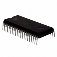
IC MCU 8K OTP 2.1MHZ 42-SDIP
Manufacturer
Freescale Semiconductor
Series
HC05r
Datasheet
1.MC68HC705C8AB.pdf
(222 pages)
Specifications of MC68HC705C8AB
Core Processor
HC05
Core Size
8-Bit
Speed
2.1MHz
Connectivity
SCI, SPI
Peripherals
POR, WDT
Number Of I /o
24
Program Memory Size
8KB (8K x 8)
Program Memory Type
OTP
Ram Size
304 x 8
Voltage - Supply (vcc/vdd)
3 V ~ 5.5 V
Oscillator Type
Internal
Operating Temperature
0°C ~ 70°C
Package / Case
42-DIP (0.600", 15.24mm)
Lead Free Status / RoHS Status
Contains lead / RoHS non-compliant
Eeprom Size
-
Data Converters
-


Serial Peripheral Interface (SPI)
11.4.2 Pin Functions in Slave Mode
Technical Data
144
Clearing the MSTR bit in the SPCR configures the SPI for operation in
slave mode. The slave-mode functions of the SPI pins are:
When CPHA = 0, the shift clock is the OR of SS with SCK. In this clock
phase mode, SS must go high between successive characters in an SPI
message. When CPHA = 1, SS may be left low for several SPI
characters. In cases with only one SPI slave MCU, the slave MCU SS
line can be tied to V
The WCOL flag bit can be improperly set when attempting the first
transmission after a reset if these conditions are present: MSTR = 0,
CPOL = 0, CPHA = 1, SS pin = 0, and SCK pin = 1. The reset states of
the CPOL and CPHA bits are 0 and 1, respectively. Under normal
operating conditions (CPOL = 0, CPHA = 1), the SCK input will be low.
The incorrect setting of the WCOL bit can be prevented in two ways:
1. Send a dummy transmission after reset, clear the WCOL flag, and
2. Use the MSTR bit in the SPCR (SPI control register). This is
•
•
•
•
Freescale Semiconductor, Inc.
For More Information On This Product,
PD4/SCK (serial clock) — In slave mode, the PD4/SCK pin is the
input for the synchronizing clock signal from the master SPI.
PD3/MOSI (master output, slave input) — In slave mode, the
PD3/MOSI pin is the serial input.
PD2/MISO (master input, slave output) — In slave mode, the
PD2/MISO pin is the serial output.
PD5/SS (slave select) — In slave mode, the PD5/SS pin enables
the SPI for data and serial clock reception from a master SPI.
then proceed with the real transmission.
accomplished by setting the MSTR bit at the same time the CPOL
and CPHA bits are programmed to the desired logic levels. Then,
the data register can be written to if desired. After this, the MSTR
bit should be set to a logic 0, the SPE (SPI enable bit) should be
set to a logic 1, and the CPOL, CPHA, SPR1, and SPR0 bits set
to the desired logic levels. If this procedure is followed after a reset
and before the first access to the SPDR, the WCOL flag will not be
set.
Serial Peripheral Interface (SPI)
Go to: www.freescale.com
SS
as long as CPHA = 1 clock modes are used.
MC68HC705C8A — Rev. 3
Related parts for MC68HC705C8AB
Image
Part Number
Description
Manufacturer
Datasheet
Request
R

Part Number:
Description:
APPENDIX A ELECTRICAL CHARACTERISTICS
Manufacturer:
FREESCALE [Freescale Semiconductor, Inc]
Datasheet:

Part Number:
Description:
Manufacturer:
Freescale Semiconductor, Inc
Datasheet:
Part Number:
Description:
Manufacturer:
Freescale Semiconductor, Inc
Datasheet:
Part Number:
Description:
Manufacturer:
Freescale Semiconductor, Inc
Datasheet:
Part Number:
Description:
Manufacturer:
Freescale Semiconductor, Inc
Datasheet:
Part Number:
Description:
Manufacturer:
Freescale Semiconductor, Inc
Datasheet:
Part Number:
Description:
Manufacturer:
Freescale Semiconductor, Inc
Datasheet:
Part Number:
Description:
Manufacturer:
Freescale Semiconductor, Inc
Datasheet:
Part Number:
Description:
Manufacturer:
Freescale Semiconductor, Inc
Datasheet:
Part Number:
Description:
Manufacturer:
Freescale Semiconductor, Inc
Datasheet:
Part Number:
Description:
Manufacturer:
Freescale Semiconductor, Inc
Datasheet:
Part Number:
Description:
Manufacturer:
Freescale Semiconductor, Inc
Datasheet:
Part Number:
Description:
Manufacturer:
Freescale Semiconductor, Inc
Datasheet:
Part Number:
Description:
Manufacturer:
Freescale Semiconductor, Inc
Datasheet:
Part Number:
Description:
Manufacturer:
Freescale Semiconductor, Inc
Datasheet: