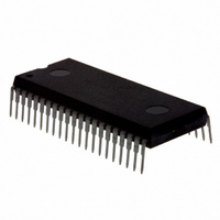
MC68HC705C8AB Freescale Semiconductor, MC68HC705C8AB Datasheet - Page 87

MC68HC705C8AB
Manufacturer Part Number
MC68HC705C8AB
Description
IC MCU 8K OTP 2.1MHZ 42-SDIP
Manufacturer
Freescale Semiconductor
Series
HC05r
Datasheet
1.MC68HC705C8AB.pdf
(222 pages)
Specifications of MC68HC705C8AB
Core Processor
HC05
Core Size
8-Bit
Speed
2.1MHz
Connectivity
SCI, SPI
Peripherals
POR, WDT
Number Of I /o
24
Program Memory Size
8KB (8K x 8)
Program Memory Type
OTP
Ram Size
304 x 8
Voltage - Supply (vcc/vdd)
3 V ~ 5.5 V
Oscillator Type
Internal
Operating Temperature
0°C ~ 70°C
Package / Case
42-DIP (0.600", 15.24mm)
Lead Free Status / RoHS Status
Contains lead / RoHS non-compliant
Eeprom Size
-
Data Converters
-
- Current page: 87 of 222
- Download datasheet (3Mb)
7.5.3 Port C Logic
MC68HC705C8A — Rev. 3
MOTOROLA
NOTE:
Figure 7-9
When a port C pin is programmed as an output, reading the port bit reads
the value of the data latch and not the voltage on the pin. When a port C
pin is programmed as an input, reading the port bit reads the voltage
level on the pin. The data latch can always be written, regardless of the
state of its DDRC bit.
pins.
To avoid excessive current draw, tie all unused input pins to V
or change I/O pins to outputs by writing to DDRC in user code as early
as possible.
1. Hi-Z = high impedance
2. Writing affects data register but does not affect input.
DDRC Bit
Freescale Semiconductor, Inc.
For More Information On This Product,
0
1
READ $0006
WRITE $0006
WRITE $0002
READ $0002
shows port C I/O logic.
Go to: www.freescale.com
I/O Pin Mode
Parallel Input/Output (I/O)
Input, Hi-Z
RESET
Output
Table 7-3. Port C Pin Functions
Figure 7-9. Port C I/O Logic
Table 7-3
(1)
DATA DIRECTION
PORT C DATA
REGISTER C
REGISTER
BIT DDRCx
BIT PCx
Accesses to DDRC
DDRC7–DDRC0
DDRC7–DDRC0
Read/Write
summarizes the operation of the port C
PC7–PC0
Parallel Input/Output (I/O)
Accesses to PORTC
Read
Pin
Technical Data
PC7–PC0
PC7–PC0
DD
Write
or V
PCx
Port C
(2)
SS
Related parts for MC68HC705C8AB
Image
Part Number
Description
Manufacturer
Datasheet
Request
R

Part Number:
Description:
APPENDIX A ELECTRICAL CHARACTERISTICS
Manufacturer:
FREESCALE [Freescale Semiconductor, Inc]
Datasheet:
Part Number:
Description:
Manufacturer:
Freescale Semiconductor, Inc
Datasheet:
Part Number:
Description:
Manufacturer:
Freescale Semiconductor, Inc
Datasheet:
Part Number:
Description:
Manufacturer:
Freescale Semiconductor, Inc
Datasheet:
Part Number:
Description:
Manufacturer:
Freescale Semiconductor, Inc
Datasheet:
Part Number:
Description:
Manufacturer:
Freescale Semiconductor, Inc
Datasheet:
Part Number:
Description:
Manufacturer:
Freescale Semiconductor, Inc
Datasheet:
Part Number:
Description:
Manufacturer:
Freescale Semiconductor, Inc
Datasheet:
Part Number:
Description:
Manufacturer:
Freescale Semiconductor, Inc
Datasheet:
Part Number:
Description:
Manufacturer:
Freescale Semiconductor, Inc
Datasheet:
Part Number:
Description:
Manufacturer:
Freescale Semiconductor, Inc
Datasheet:
Part Number:
Description:
Manufacturer:
Freescale Semiconductor, Inc
Datasheet:
Part Number:
Description:
Manufacturer:
Freescale Semiconductor, Inc
Datasheet:
Part Number:
Description:
Manufacturer:
Freescale Semiconductor, Inc
Datasheet:
Part Number:
Description:
Manufacturer:
Freescale Semiconductor, Inc
Datasheet:


